K. Bharathi, K. Chandra Babu Naidu, Eshwarappa Veena, Madunuri Chandrasekhar, D. Baba Basha, L. Siva Sankara Reddy
{"title":"AlxNi1−xTiO3+δ (x = 0.2-0.8)纳米材料的介电吸收应用","authors":"K. Bharathi, K. Chandra Babu Naidu, Eshwarappa Veena, Madunuri Chandrasekhar, D. Baba Basha, L. Siva Sankara Reddy","doi":"10.1007/s10854-025-15598-x","DOIUrl":null,"url":null,"abstract":"<div><p>The Al<sub><i>x</i></sub>Ni<sub>1−<i>x</i></sub>TiO<sub>3+δ</sub> (<i>x</i> = 0.2, 0.4, 0.6 & 0.8) (ANT) nanoparticles are synthesized via hydrothermal method. The X-ray diffraction patterns reveal the tetragonal structure having few secondary phase structures. The crystallite size ‘D’ value is varying unsystematically between 51.14 ± 0.914 and 66.32 ± 0.384 nm as a function of Al-content. The W–H plots are drawn to find the internal microstrain. The microstructure shows the clustered nature of ANT revealing the existence of interactions among the nanoparticles. The optical bandgap (<i>E</i><sub>g</sub>) values are determined using Tauc’s plots and decreasing with an increase of Al-content. The high dielectric constant, and loss values are noted for <i>x</i> = 0.2, and for <i>x</i> = 0.4–0.6, a little less magnitude (as compared to <i>x</i> = 0.2) is noted. These lossy materials may be suggested for the microwave dielectric absorber applications in the fields of electronics and energy. The electrical conduction mechanism is illustrated by means of dielectric modulus, ac-electrical conductivity, and impedance analysis. The impedance analysis provides the low grain (<i>R</i><sub>g</sub> ~ 29,410.7 Ω) and the high grain boundary (<i>R</i><sub>gb</sub> ~ 47,065.8 Ω) resistance values for x = 0.4. The bulk conductivity values (for <i>x</i> = 0.4) are noted to be 5.411 × 10<sup>–6</sup> S/cm & 3.381 × 10<sup>–6</sup> S/cm as the contributions of grain and grain boundaries, respectively.</p></div>","PeriodicalId":646,"journal":{"name":"Journal of Materials Science: Materials in Electronics","volume":"36 24","pages":""},"PeriodicalIF":2.8000,"publicationDate":"2025-08-25","publicationTypes":"Journal Article","fieldsOfStudy":null,"isOpenAccess":false,"openAccessPdf":"","citationCount":"0","resultStr":"{\"title\":\"AlxNi1−xTiO3+δ (x = 0.2–0.8) nanomaterials for dielectric absorber applications\",\"authors\":\"K. Bharathi, K. Chandra Babu Naidu, Eshwarappa Veena, Madunuri Chandrasekhar, D. Baba Basha, L. Siva Sankara Reddy\",\"doi\":\"10.1007/s10854-025-15598-x\",\"DOIUrl\":null,\"url\":null,\"abstract\":\"<div><p>The Al<sub><i>x</i></sub>Ni<sub>1−<i>x</i></sub>TiO<sub>3+δ</sub> (<i>x</i> = 0.2, 0.4, 0.6 & 0.8) (ANT) nanoparticles are synthesized via hydrothermal method. The X-ray diffraction patterns reveal the tetragonal structure having few secondary phase structures. The crystallite size ‘D’ value is varying unsystematically between 51.14 ± 0.914 and 66.32 ± 0.384 nm as a function of Al-content. The W–H plots are drawn to find the internal microstrain. The microstructure shows the clustered nature of ANT revealing the existence of interactions among the nanoparticles. The optical bandgap (<i>E</i><sub>g</sub>) values are determined using Tauc’s plots and decreasing with an increase of Al-content. The high dielectric constant, and loss values are noted for <i>x</i> = 0.2, and for <i>x</i> = 0.4–0.6, a little less magnitude (as compared to <i>x</i> = 0.2) is noted. These lossy materials may be suggested for the microwave dielectric absorber applications in the fields of electronics and energy. The electrical conduction mechanism is illustrated by means of dielectric modulus, ac-electrical conductivity, and impedance analysis. The impedance analysis provides the low grain (<i>R</i><sub>g</sub> ~ 29,410.7 Ω) and the high grain boundary (<i>R</i><sub>gb</sub> ~ 47,065.8 Ω) resistance values for x = 0.4. The bulk conductivity values (for <i>x</i> = 0.4) are noted to be 5.411 × 10<sup>–6</sup> S/cm & 3.381 × 10<sup>–6</sup> S/cm as the contributions of grain and grain boundaries, respectively.</p></div>\",\"PeriodicalId\":646,\"journal\":{\"name\":\"Journal of Materials Science: Materials in Electronics\",\"volume\":\"36 24\",\"pages\":\"\"},\"PeriodicalIF\":2.8000,\"publicationDate\":\"2025-08-25\",\"publicationTypes\":\"Journal Article\",\"fieldsOfStudy\":null,\"isOpenAccess\":false,\"openAccessPdf\":\"\",\"citationCount\":\"0\",\"resultStr\":null,\"platform\":\"Semanticscholar\",\"paperid\":null,\"PeriodicalName\":\"Journal of Materials Science: Materials in Electronics\",\"FirstCategoryId\":\"5\",\"ListUrlMain\":\"https://link.springer.com/article/10.1007/s10854-025-15598-x\",\"RegionNum\":4,\"RegionCategory\":\"工程技术\",\"ArticlePicture\":[],\"TitleCN\":null,\"AbstractTextCN\":null,\"PMCID\":null,\"EPubDate\":\"\",\"PubModel\":\"\",\"JCR\":\"Q2\",\"JCRName\":\"ENGINEERING, ELECTRICAL & ELECTRONIC\",\"Score\":null,\"Total\":0}","platform":"Semanticscholar","paperid":null,"PeriodicalName":"Journal of Materials Science: Materials in Electronics","FirstCategoryId":"5","ListUrlMain":"https://link.springer.com/article/10.1007/s10854-025-15598-x","RegionNum":4,"RegionCategory":"工程技术","ArticlePicture":[],"TitleCN":null,"AbstractTextCN":null,"PMCID":null,"EPubDate":"","PubModel":"","JCR":"Q2","JCRName":"ENGINEERING, ELECTRICAL & ELECTRONIC","Score":null,"Total":0}
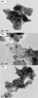
AlxNi1−xTiO3+δ (x = 0.2–0.8) nanomaterials for dielectric absorber applications
The AlxNi1−xTiO3+δ (x = 0.2, 0.4, 0.6 & 0.8) (ANT) nanoparticles are synthesized via hydrothermal method. The X-ray diffraction patterns reveal the tetragonal structure having few secondary phase structures. The crystallite size ‘D’ value is varying unsystematically between 51.14 ± 0.914 and 66.32 ± 0.384 nm as a function of Al-content. The W–H plots are drawn to find the internal microstrain. The microstructure shows the clustered nature of ANT revealing the existence of interactions among the nanoparticles. The optical bandgap (Eg) values are determined using Tauc’s plots and decreasing with an increase of Al-content. The high dielectric constant, and loss values are noted for x = 0.2, and for x = 0.4–0.6, a little less magnitude (as compared to x = 0.2) is noted. These lossy materials may be suggested for the microwave dielectric absorber applications in the fields of electronics and energy. The electrical conduction mechanism is illustrated by means of dielectric modulus, ac-electrical conductivity, and impedance analysis. The impedance analysis provides the low grain (Rg ~ 29,410.7 Ω) and the high grain boundary (Rgb ~ 47,065.8 Ω) resistance values for x = 0.4. The bulk conductivity values (for x = 0.4) are noted to be 5.411 × 10⁻⁶ S/cm & 3.381 × 10⁻⁶ S/cm as the contributions of grain and grain boundaries, respectively.
期刊介绍:
The Journal of Materials Science: Materials in Electronics is an established refereed companion to the Journal of Materials Science. It publishes papers on materials and their applications in modern electronics, covering the ground between fundamental science, such as semiconductor physics, and work concerned specifically with applications. It explores the growth and preparation of new materials, as well as their processing, fabrication, bonding and encapsulation, together with the reliability, failure analysis, quality assurance and characterization related to the whole range of applications in electronics. The Journal presents papers in newly developing fields such as low dimensional structures and devices, optoelectronics including III-V compounds, glasses and linear/non-linear crystal materials and lasers, high Tc superconductors, conducting polymers, thick film materials and new contact technologies, as well as the established electronics device and circuit materials.

 求助内容:
求助内容: 应助结果提醒方式:


