Yu-Wu Wang*, Kaushlendra Agrahari, Jiann-Heng Chen*, Zih-Wei Ye, Wen-Ting Wang, Hsuan-Jui Ou, Chun-Ying Huang and Sun-Zen Chen,
{"title":"溶液处理氧化铟和纳米压印转移技术实现高灵敏度isfet","authors":"Yu-Wu Wang*, Kaushlendra Agrahari, Jiann-Heng Chen*, Zih-Wei Ye, Wen-Ting Wang, Hsuan-Jui Ou, Chun-Ying Huang and Sun-Zen Chen, ","doi":"10.1021/acsaelm.5c00946","DOIUrl":null,"url":null,"abstract":"<p >This study presents a facile approach for fabricating high-performance indium oxide (In<sub>2</sub>O<sub>3</sub>) nanosheet thin-film transistors (TFTs) by using a combination of solution processing and nanoimprint transfer techniques. For the first time, nanostructured In<sub>2</sub>O<sub>3</sub>─featuring nanowire and honeycomb patterns with line widths as narrow as ∼158 and ∼89 nm, respectively─was successfully realized via a sol–gel nanoimprint strategy. The resulting nanosheet TFTs demonstrated outstanding electrical characteristics, including sharp output current profiles, a high ON/OFF current ratio, and enhanced field-effect mobility. By exploiting the advantages of nanoscale patterning and capacitive coupling in double-gate structures, the study further introduces ultrasensitive In<sub>2</sub>O<sub>3</sub>-based ion-sensitive field-effect transistors (ISFETs) for pH sensing, achieving a remarkable sensitivity of approximately −84.1 mV/pH. These findings not only highlight the potential of scalable nanofabrication techniques for oxide electronics but also open exciting opportunities for next-generation biomedical sensors and wearable electronic systems.</p>","PeriodicalId":3,"journal":{"name":"ACS Applied Electronic Materials","volume":"7 16","pages":"7631–7639"},"PeriodicalIF":4.7000,"publicationDate":"2025-08-12","publicationTypes":"Journal Article","fieldsOfStudy":null,"isOpenAccess":false,"openAccessPdf":"","citationCount":"0","resultStr":"{\"title\":\"High-Sensitivity ISFETs Enabled by Solution-Processed Indium Oxide and Nanoimprint Transferring Techniques\",\"authors\":\"Yu-Wu Wang*, Kaushlendra Agrahari, Jiann-Heng Chen*, Zih-Wei Ye, Wen-Ting Wang, Hsuan-Jui Ou, Chun-Ying Huang and Sun-Zen Chen, \",\"doi\":\"10.1021/acsaelm.5c00946\",\"DOIUrl\":null,\"url\":null,\"abstract\":\"<p >This study presents a facile approach for fabricating high-performance indium oxide (In<sub>2</sub>O<sub>3</sub>) nanosheet thin-film transistors (TFTs) by using a combination of solution processing and nanoimprint transfer techniques. For the first time, nanostructured In<sub>2</sub>O<sub>3</sub>─featuring nanowire and honeycomb patterns with line widths as narrow as ∼158 and ∼89 nm, respectively─was successfully realized via a sol–gel nanoimprint strategy. The resulting nanosheet TFTs demonstrated outstanding electrical characteristics, including sharp output current profiles, a high ON/OFF current ratio, and enhanced field-effect mobility. By exploiting the advantages of nanoscale patterning and capacitive coupling in double-gate structures, the study further introduces ultrasensitive In<sub>2</sub>O<sub>3</sub>-based ion-sensitive field-effect transistors (ISFETs) for pH sensing, achieving a remarkable sensitivity of approximately −84.1 mV/pH. These findings not only highlight the potential of scalable nanofabrication techniques for oxide electronics but also open exciting opportunities for next-generation biomedical sensors and wearable electronic systems.</p>\",\"PeriodicalId\":3,\"journal\":{\"name\":\"ACS Applied Electronic Materials\",\"volume\":\"7 16\",\"pages\":\"7631–7639\"},\"PeriodicalIF\":4.7000,\"publicationDate\":\"2025-08-12\",\"publicationTypes\":\"Journal Article\",\"fieldsOfStudy\":null,\"isOpenAccess\":false,\"openAccessPdf\":\"\",\"citationCount\":\"0\",\"resultStr\":null,\"platform\":\"Semanticscholar\",\"paperid\":null,\"PeriodicalName\":\"ACS Applied Electronic Materials\",\"FirstCategoryId\":\"88\",\"ListUrlMain\":\"https://pubs.acs.org/doi/10.1021/acsaelm.5c00946\",\"RegionNum\":3,\"RegionCategory\":\"材料科学\",\"ArticlePicture\":[],\"TitleCN\":null,\"AbstractTextCN\":null,\"PMCID\":null,\"EPubDate\":\"\",\"PubModel\":\"\",\"JCR\":\"Q1\",\"JCRName\":\"ENGINEERING, ELECTRICAL & ELECTRONIC\",\"Score\":null,\"Total\":0}","platform":"Semanticscholar","paperid":null,"PeriodicalName":"ACS Applied Electronic Materials","FirstCategoryId":"88","ListUrlMain":"https://pubs.acs.org/doi/10.1021/acsaelm.5c00946","RegionNum":3,"RegionCategory":"材料科学","ArticlePicture":[],"TitleCN":null,"AbstractTextCN":null,"PMCID":null,"EPubDate":"","PubModel":"","JCR":"Q1","JCRName":"ENGINEERING, ELECTRICAL & ELECTRONIC","Score":null,"Total":0}
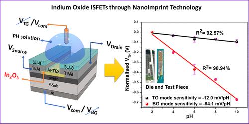
High-Sensitivity ISFETs Enabled by Solution-Processed Indium Oxide and Nanoimprint Transferring Techniques
This study presents a facile approach for fabricating high-performance indium oxide (In2O3) nanosheet thin-film transistors (TFTs) by using a combination of solution processing and nanoimprint transfer techniques. For the first time, nanostructured In2O3─featuring nanowire and honeycomb patterns with line widths as narrow as ∼158 and ∼89 nm, respectively─was successfully realized via a sol–gel nanoimprint strategy. The resulting nanosheet TFTs demonstrated outstanding electrical characteristics, including sharp output current profiles, a high ON/OFF current ratio, and enhanced field-effect mobility. By exploiting the advantages of nanoscale patterning and capacitive coupling in double-gate structures, the study further introduces ultrasensitive In2O3-based ion-sensitive field-effect transistors (ISFETs) for pH sensing, achieving a remarkable sensitivity of approximately −84.1 mV/pH. These findings not only highlight the potential of scalable nanofabrication techniques for oxide electronics but also open exciting opportunities for next-generation biomedical sensors and wearable electronic systems.
期刊介绍:
ACS Applied Electronic Materials is an interdisciplinary journal publishing original research covering all aspects of electronic materials. The journal is devoted to reports of new and original experimental and theoretical research of an applied nature that integrate knowledge in the areas of materials science, engineering, optics, physics, and chemistry into important applications of electronic materials. Sample research topics that span the journal's scope are inorganic, organic, ionic and polymeric materials with properties that include conducting, semiconducting, superconducting, insulating, dielectric, magnetic, optoelectronic, piezoelectric, ferroelectric and thermoelectric.
Indexed/Abstracted:
Web of Science SCIE
Scopus
CAS
INSPEC
Portico

 求助内容:
求助内容: 应助结果提醒方式:


