{"title":"1位20T-HyDGFA超低功耗高速设计分析","authors":"Ramsha Suhail, Pragya Srivastava, Richa Yadav, K. Pradnya, Ridhima Choudhary, Priya Singh, Prachi Yadav","doi":"10.1007/s10470-025-02470-5","DOIUrl":null,"url":null,"abstract":"<div><p>In the age of fast digital communication, the use of portable devices is significantly increasing. Given their compact size, it is essential for these devices to fulfill the technological requirements of reduced power consumption, minimal area, and high speed. The 1-bit full adder cell is a critical functional unit in the computational industry. This paper presents a new hybrid methodology for designing 20 transistor full adder (FA) based on Double Gate MOSFET (20T-HyDGFA). The proposed circuit is designed to optimize the balance between propagation delay (T<sub><b><i>d</i></b></sub>) and power consumption (PWR), therefore enhancing efficiency in the IC sector. This study compares the proposed circuit with existing FA circuits and measures numerous performance metrics, including T<sub><b><i>d</i></b></sub>, PWR, Power Delay Product (PDP), Energy Delay Product (EDP), Energy-Delay² Product (ED<sup>2</sup>P), and noise margin. Operated at a supply voltage (V<sub><b><i>DD</i></b></sub>) of 0.5 V, the proposed design exhibits a notably low PWR of 0.98nW (1.18x), with a remarkably short T<sub><b><i>d</i></b></sub> of 19.30ps (20.63x), accompanied by a substantial PDP of 0.02 aJ (24.22x), EDP of 0.36 aJ-ns (500.22x) and ED<sup>2</sup>P of 6.21 aJ-ps<sup>2</sup> (1150x) as simulated on HSPICE software at a 16 nm technology node. A detailed, Monte Carlo Simulation is conducted for the proposed FA circuit to validate the obtained results and then compared with the existing best state-of-the-art FA circuits. Furthermore, this paper introduces an application, 4-Bit Ripple Carry Adder (RCA), using the proposed 20T-HyDGFA Circuit (4-HyDGRCA). The physical layout design is facilitated by the enhanced results, which occupy an optimized area of 9.3µm<sup>2</sup> and 41.9 µm<sup>2</sup> for the proposed circuit and proposed application circuit, respectively.</p></div>","PeriodicalId":7827,"journal":{"name":"Analog Integrated Circuits and Signal Processing","volume":"125 1","pages":""},"PeriodicalIF":1.4000,"publicationDate":"2025-08-22","publicationTypes":"Journal Article","fieldsOfStudy":null,"isOpenAccess":false,"openAccessPdf":"","citationCount":"0","resultStr":"{\"title\":\"Ultra-Low Power and High-Speed Design Analysis of 1-Bit 20T-HyDGFA using a Dual-Gate Domino Inverter\",\"authors\":\"Ramsha Suhail, Pragya Srivastava, Richa Yadav, K. Pradnya, Ridhima Choudhary, Priya Singh, Prachi Yadav\",\"doi\":\"10.1007/s10470-025-02470-5\",\"DOIUrl\":null,\"url\":null,\"abstract\":\"<div><p>In the age of fast digital communication, the use of portable devices is significantly increasing. Given their compact size, it is essential for these devices to fulfill the technological requirements of reduced power consumption, minimal area, and high speed. The 1-bit full adder cell is a critical functional unit in the computational industry. This paper presents a new hybrid methodology for designing 20 transistor full adder (FA) based on Double Gate MOSFET (20T-HyDGFA). The proposed circuit is designed to optimize the balance between propagation delay (T<sub><b><i>d</i></b></sub>) and power consumption (PWR), therefore enhancing efficiency in the IC sector. This study compares the proposed circuit with existing FA circuits and measures numerous performance metrics, including T<sub><b><i>d</i></b></sub>, PWR, Power Delay Product (PDP), Energy Delay Product (EDP), Energy-Delay² Product (ED<sup>2</sup>P), and noise margin. Operated at a supply voltage (V<sub><b><i>DD</i></b></sub>) of 0.5 V, the proposed design exhibits a notably low PWR of 0.98nW (1.18x), with a remarkably short T<sub><b><i>d</i></b></sub> of 19.30ps (20.63x), accompanied by a substantial PDP of 0.02 aJ (24.22x), EDP of 0.36 aJ-ns (500.22x) and ED<sup>2</sup>P of 6.21 aJ-ps<sup>2</sup> (1150x) as simulated on HSPICE software at a 16 nm technology node. A detailed, Monte Carlo Simulation is conducted for the proposed FA circuit to validate the obtained results and then compared with the existing best state-of-the-art FA circuits. Furthermore, this paper introduces an application, 4-Bit Ripple Carry Adder (RCA), using the proposed 20T-HyDGFA Circuit (4-HyDGRCA). The physical layout design is facilitated by the enhanced results, which occupy an optimized area of 9.3µm<sup>2</sup> and 41.9 µm<sup>2</sup> for the proposed circuit and proposed application circuit, respectively.</p></div>\",\"PeriodicalId\":7827,\"journal\":{\"name\":\"Analog Integrated Circuits and Signal Processing\",\"volume\":\"125 1\",\"pages\":\"\"},\"PeriodicalIF\":1.4000,\"publicationDate\":\"2025-08-22\",\"publicationTypes\":\"Journal Article\",\"fieldsOfStudy\":null,\"isOpenAccess\":false,\"openAccessPdf\":\"\",\"citationCount\":\"0\",\"resultStr\":null,\"platform\":\"Semanticscholar\",\"paperid\":null,\"PeriodicalName\":\"Analog Integrated Circuits and Signal Processing\",\"FirstCategoryId\":\"5\",\"ListUrlMain\":\"https://link.springer.com/article/10.1007/s10470-025-02470-5\",\"RegionNum\":4,\"RegionCategory\":\"工程技术\",\"ArticlePicture\":[],\"TitleCN\":null,\"AbstractTextCN\":null,\"PMCID\":null,\"EPubDate\":\"\",\"PubModel\":\"\",\"JCR\":\"Q4\",\"JCRName\":\"COMPUTER SCIENCE, HARDWARE & ARCHITECTURE\",\"Score\":null,\"Total\":0}","platform":"Semanticscholar","paperid":null,"PeriodicalName":"Analog Integrated Circuits and Signal Processing","FirstCategoryId":"5","ListUrlMain":"https://link.springer.com/article/10.1007/s10470-025-02470-5","RegionNum":4,"RegionCategory":"工程技术","ArticlePicture":[],"TitleCN":null,"AbstractTextCN":null,"PMCID":null,"EPubDate":"","PubModel":"","JCR":"Q4","JCRName":"COMPUTER SCIENCE, HARDWARE & ARCHITECTURE","Score":null,"Total":0}
Ultra-Low Power and High-Speed Design Analysis of 1-Bit 20T-HyDGFA using a Dual-Gate Domino Inverter
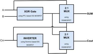
In the age of fast digital communication, the use of portable devices is significantly increasing. Given their compact size, it is essential for these devices to fulfill the technological requirements of reduced power consumption, minimal area, and high speed. The 1-bit full adder cell is a critical functional unit in the computational industry. This paper presents a new hybrid methodology for designing 20 transistor full adder (FA) based on Double Gate MOSFET (20T-HyDGFA). The proposed circuit is designed to optimize the balance between propagation delay (Td) and power consumption (PWR), therefore enhancing efficiency in the IC sector. This study compares the proposed circuit with existing FA circuits and measures numerous performance metrics, including Td, PWR, Power Delay Product (PDP), Energy Delay Product (EDP), Energy-Delay² Product (ED2P), and noise margin. Operated at a supply voltage (VDD) of 0.5 V, the proposed design exhibits a notably low PWR of 0.98nW (1.18x), with a remarkably short Td of 19.30ps (20.63x), accompanied by a substantial PDP of 0.02 aJ (24.22x), EDP of 0.36 aJ-ns (500.22x) and ED2P of 6.21 aJ-ps2 (1150x) as simulated on HSPICE software at a 16 nm technology node. A detailed, Monte Carlo Simulation is conducted for the proposed FA circuit to validate the obtained results and then compared with the existing best state-of-the-art FA circuits. Furthermore, this paper introduces an application, 4-Bit Ripple Carry Adder (RCA), using the proposed 20T-HyDGFA Circuit (4-HyDGRCA). The physical layout design is facilitated by the enhanced results, which occupy an optimized area of 9.3µm2 and 41.9 µm2 for the proposed circuit and proposed application circuit, respectively.
期刊介绍:
Analog Integrated Circuits and Signal Processing is an archival peer reviewed journal dedicated to the design and application of analog, radio frequency (RF), and mixed signal integrated circuits (ICs) as well as signal processing circuits and systems. It features both new research results and tutorial views and reflects the large volume of cutting-edge research activity in the worldwide field today.
A partial list of topics includes analog and mixed signal interface circuits and systems; analog and RFIC design; data converters; active-RC, switched-capacitor, and continuous-time integrated filters; mixed analog/digital VLSI systems; wireless radio transceivers; clock and data recovery circuits; and high speed optoelectronic circuits and systems.

 求助内容:
求助内容: 应助结果提醒方式:


