采用磁控溅射Sb和后硫化法制备Sb2S3薄膜太阳能电池
IF 7.9
2区 材料科学
Q1 MATERIALS SCIENCE, MULTIDISCIPLINARY
引用次数: 0
摘要
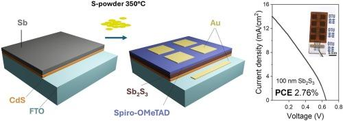
本研究探索了采用射频磁控溅射锑(Sb)并进行硫化的方法制备和优化超层结构硫化锑(Sb2S3)薄膜太阳能电池。系统研究了不同吸收层厚度和缓冲层厚度对FTO/CdS/Sb2S3/Spiro-OMeTAD/Au太阳能电池器件光电性能的影响。分析技术证实了经Sb后硫化得到的Sb2S3膜的结构和化学性质,表明结晶度得到改善,组成与Sb2S3相一致。将Sb2S3吸收体厚度优化至100 nm后,该器件的最大功率转换效率为2.76%,短路电流密度(Jsc)提高至14 mA/cm2,开路电压(Voc)提高至650 mV。该器件在380-740 nm波长范围内显示出高达20%的半透明,使其适合室内和建筑集成光伏应用。这些结果强调了磁控溅射Sb2S3在新兴透明薄膜光伏电池中的潜力,同时强调了厚度控制和界面工程对提高效率的重要性。本文章由计算机程序翻译,如有差异,请以英文原文为准。
Superstrate structured Sb2S3 thin-film solar cells by magnetron sputtering of Sb and post-sulfurization
This study explores the fabrication and optimization of superstrate-structured antimony sulfide (Sb2S3) thin-film solar cells using RF magnetron sputtering of antimony (Sb) followed by sulfurization. The study systematically investigates the effects of varying absorber and buffer layer thicknesses on the photovoltaic performance of FTO/CdS/Sb2S3/Spiro-OMeTAD/Au solar cell devices. Analytical techniques confirmed the structural and chemical properties of the Sb2S3 films obtained after Sb post-sulfurization, demonstrating improved crystallinity and a composition consistent with a primarily Sb2S3 phase. Optimizing the Sb2S3 absorber thickness to 100 nm resulted in a maximum power conversion efficiency of the champion device of 2.76%, with enhanced short-circuit current density (Jsc) up to 14 mA/cm2 and open-circuit voltage (Voc) of up to 650 mV. The device exhibited semi-transparency up to 20% in the wavelength range of 380–740 nm, making it suitable for indoor and building-integrated photovoltaic applications. The results underscore the potential of magnetron-sputtered Sb2S3 for emerging transparent thin-film photovoltaics while highlighting the importance of thickness control and interface engineering for efficiency improvements.
求助全文
通过发布文献求助,成功后即可免费获取论文全文。
去求助
来源期刊
Materials & Design
Engineering-Mechanical Engineering
CiteScore
14.30
自引率
7.10%
发文量
1028
审稿时长
85 days
期刊介绍:
Materials and Design is a multi-disciplinary journal that publishes original research reports, review articles, and express communications. The journal focuses on studying the structure and properties of inorganic and organic materials, advancements in synthesis, processing, characterization, and testing, the design of materials and engineering systems, and their applications in technology. It aims to bring together various aspects of materials science, engineering, physics, and chemistry.
The journal explores themes ranging from materials to design and aims to reveal the connections between natural and artificial materials, as well as experiment and modeling. Manuscripts submitted to Materials and Design should contain elements of discovery and surprise, as they often contribute new insights into the architecture and function of matter.
 求助内容:
求助内容: 应助结果提醒方式:


