{"title":"衬底工程调节的非易失性均匀InSe晶体管。","authors":"Tieying Ma, Yunchi Wang, Guojin Feng, Haibo Shu*, Jiawei Zhang*, Yu Zhou, Dong Zhou and Yu Lin*, ","doi":"10.1021/acsnano.5c09584","DOIUrl":null,"url":null,"abstract":"<p >This study proposes a polarity regulation in two-dimensional InSe via substrate engineering. By selecting different substrates (h-BN and multilayer graphene (MLG)/SiO<sub>2</sub>), controllable doping of p-type and n-type regions on the same piece of two-dimensional InSe material is achieved. Utilizing this characteristic, a high-performance homogeneous PN junction is constructed. The rectification characteristics of this device can be dynamically regulated by the gate voltage and laser irradiation. The gate voltage can adjust the rectification ratio from 10 to more than 10<sup>7</sup>, and the regulation range and performance are significantly superior to those of the reported devices of the same kind. The rectification ratio can be effectively regulated by a broadband laser with a wavelength range of 280–965 nm. When the device is irradiated by a laser with a wavelength of 365 nm at a power of 16.75 mW/cm<sup>2</sup>, the rectification effect of the device disappears completely. Additionally, an NMOS is constructed in the n–p–n region and a PMOS is constructed in the p–n–p region on InSe respectively, and their output transfer characteristics can also be cooperatively regulated by the gate voltage and laser. Compared with traditional field induced carriers, this doping method has the advantage of nonvolatility. The doping state will not disappear with the removal of the gate voltage, which avoids the problems related to the stability during the device operation and continuous power supply. It shows important application potential in the fields of optoelectronic integration and reconfigurable electronics.</p>","PeriodicalId":21,"journal":{"name":"ACS Nano","volume":"19 34","pages":"31126–31134"},"PeriodicalIF":16.0000,"publicationDate":"2025-08-19","publicationTypes":"Journal Article","fieldsOfStudy":null,"isOpenAccess":false,"openAccessPdf":"","citationCount":"0","resultStr":"{\"title\":\"Nonvolatile Homogeneous InSe Transistors Regulated by Substrate Engineering\",\"authors\":\"Tieying Ma, Yunchi Wang, Guojin Feng, Haibo Shu*, Jiawei Zhang*, Yu Zhou, Dong Zhou and Yu Lin*, \",\"doi\":\"10.1021/acsnano.5c09584\",\"DOIUrl\":null,\"url\":null,\"abstract\":\"<p >This study proposes a polarity regulation in two-dimensional InSe via substrate engineering. By selecting different substrates (h-BN and multilayer graphene (MLG)/SiO<sub>2</sub>), controllable doping of p-type and n-type regions on the same piece of two-dimensional InSe material is achieved. Utilizing this characteristic, a high-performance homogeneous PN junction is constructed. The rectification characteristics of this device can be dynamically regulated by the gate voltage and laser irradiation. The gate voltage can adjust the rectification ratio from 10 to more than 10<sup>7</sup>, and the regulation range and performance are significantly superior to those of the reported devices of the same kind. The rectification ratio can be effectively regulated by a broadband laser with a wavelength range of 280–965 nm. When the device is irradiated by a laser with a wavelength of 365 nm at a power of 16.75 mW/cm<sup>2</sup>, the rectification effect of the device disappears completely. Additionally, an NMOS is constructed in the n–p–n region and a PMOS is constructed in the p–n–p region on InSe respectively, and their output transfer characteristics can also be cooperatively regulated by the gate voltage and laser. Compared with traditional field induced carriers, this doping method has the advantage of nonvolatility. The doping state will not disappear with the removal of the gate voltage, which avoids the problems related to the stability during the device operation and continuous power supply. It shows important application potential in the fields of optoelectronic integration and reconfigurable electronics.</p>\",\"PeriodicalId\":21,\"journal\":{\"name\":\"ACS Nano\",\"volume\":\"19 34\",\"pages\":\"31126–31134\"},\"PeriodicalIF\":16.0000,\"publicationDate\":\"2025-08-19\",\"publicationTypes\":\"Journal Article\",\"fieldsOfStudy\":null,\"isOpenAccess\":false,\"openAccessPdf\":\"\",\"citationCount\":\"0\",\"resultStr\":null,\"platform\":\"Semanticscholar\",\"paperid\":null,\"PeriodicalName\":\"ACS Nano\",\"FirstCategoryId\":\"88\",\"ListUrlMain\":\"https://pubs.acs.org/doi/10.1021/acsnano.5c09584\",\"RegionNum\":1,\"RegionCategory\":\"材料科学\",\"ArticlePicture\":[],\"TitleCN\":null,\"AbstractTextCN\":null,\"PMCID\":null,\"EPubDate\":\"\",\"PubModel\":\"\",\"JCR\":\"Q1\",\"JCRName\":\"CHEMISTRY, MULTIDISCIPLINARY\",\"Score\":null,\"Total\":0}","platform":"Semanticscholar","paperid":null,"PeriodicalName":"ACS Nano","FirstCategoryId":"88","ListUrlMain":"https://pubs.acs.org/doi/10.1021/acsnano.5c09584","RegionNum":1,"RegionCategory":"材料科学","ArticlePicture":[],"TitleCN":null,"AbstractTextCN":null,"PMCID":null,"EPubDate":"","PubModel":"","JCR":"Q1","JCRName":"CHEMISTRY, MULTIDISCIPLINARY","Score":null,"Total":0}
Nonvolatile Homogeneous InSe Transistors Regulated by Substrate Engineering
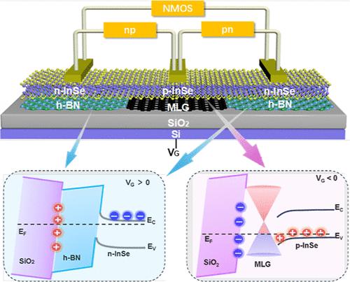
This study proposes a polarity regulation in two-dimensional InSe via substrate engineering. By selecting different substrates (h-BN and multilayer graphene (MLG)/SiO2), controllable doping of p-type and n-type regions on the same piece of two-dimensional InSe material is achieved. Utilizing this characteristic, a high-performance homogeneous PN junction is constructed. The rectification characteristics of this device can be dynamically regulated by the gate voltage and laser irradiation. The gate voltage can adjust the rectification ratio from 10 to more than 107, and the regulation range and performance are significantly superior to those of the reported devices of the same kind. The rectification ratio can be effectively regulated by a broadband laser with a wavelength range of 280–965 nm. When the device is irradiated by a laser with a wavelength of 365 nm at a power of 16.75 mW/cm2, the rectification effect of the device disappears completely. Additionally, an NMOS is constructed in the n–p–n region and a PMOS is constructed in the p–n–p region on InSe respectively, and their output transfer characteristics can also be cooperatively regulated by the gate voltage and laser. Compared with traditional field induced carriers, this doping method has the advantage of nonvolatility. The doping state will not disappear with the removal of the gate voltage, which avoids the problems related to the stability during the device operation and continuous power supply. It shows important application potential in the fields of optoelectronic integration and reconfigurable electronics.
期刊介绍:
ACS Nano, published monthly, serves as an international forum for comprehensive articles on nanoscience and nanotechnology research at the intersections of chemistry, biology, materials science, physics, and engineering. The journal fosters communication among scientists in these communities, facilitating collaboration, new research opportunities, and advancements through discoveries. ACS Nano covers synthesis, assembly, characterization, theory, and simulation of nanostructures, nanobiotechnology, nanofabrication, methods and tools for nanoscience and nanotechnology, and self- and directed-assembly. Alongside original research articles, it offers thorough reviews, perspectives on cutting-edge research, and discussions envisioning the future of nanoscience and nanotechnology.

 求助内容:
求助内容: 应助结果提醒方式:


