预算友好型纳米制造:来自高压直流和化学蚀刻的多孔结构

IF 3.1 4区 物理与天体物理 Q3 MATERIALS SCIENCE, MULTIDISCIPLINARY
S.E. García , M.A. Salguero Salas , D.M. Arciniegas Jaimes , M.I. Broens , S.M. Molina , E.A. Romero , O.E. Linarez Pérez , V.C. Fuertes , N. Bajales
{"title":"预算友好型纳米制造:来自高压直流和化学蚀刻的多孔结构","authors":"S.E. García ,&nbsp;M.A. Salguero Salas ,&nbsp;D.M. Arciniegas Jaimes ,&nbsp;M.I. Broens ,&nbsp;S.M. Molina ,&nbsp;E.A. Romero ,&nbsp;O.E. Linarez Pérez ,&nbsp;V.C. Fuertes ,&nbsp;N. Bajales","doi":"10.1016/j.cap.2025.08.008","DOIUrl":null,"url":null,"abstract":"<div><div>Anodic materials provide a versatile platform for nanotechnological developments due to their customizable properties. Our work presents a cost-effective, user-friendly approach for fabricating high-quality anodic materials through hard anodization (HA), which is one of the most widely used techniques for efficiently fabricating anodic aluminum oxide (AAO) platforms in short times by applying high voltage. We developed a configurable power supply with a simple topology that can reach up to 190 V, which management was achieved by a basic processor board. In addition, we implemented a monitoring system for acquiring process anodization parameters. This approach significantly reduces the cost barrier associated with traditional methods, like induction-based power supplies. To demonstrate the effectiveness of our strategic experimental setup, we have successfully fabricated AAO templates to be used as substrates for surface-enhanced Raman spectroscopy (SERS). Thus, our low-cost modular friendly experimental setup offers a promising avenue for creating well-defined nanostructures with broad applications in nanotechnology.</div></div>","PeriodicalId":11037,"journal":{"name":"Current Applied Physics","volume":"79 ","pages":"Pages 104-111"},"PeriodicalIF":3.1000,"publicationDate":"2025-08-13","publicationTypes":"Journal Article","fieldsOfStudy":null,"isOpenAccess":false,"openAccessPdf":"","citationCount":"0","resultStr":"{\"title\":\"Budget-friendly nanofabrication: Porous structures from high voltage DC and chemical etching\",\"authors\":\"S.E. García ,&nbsp;M.A. Salguero Salas ,&nbsp;D.M. Arciniegas Jaimes ,&nbsp;M.I. Broens ,&nbsp;S.M. Molina ,&nbsp;E.A. Romero ,&nbsp;O.E. Linarez Pérez ,&nbsp;V.C. Fuertes ,&nbsp;N. Bajales\",\"doi\":\"10.1016/j.cap.2025.08.008\",\"DOIUrl\":null,\"url\":null,\"abstract\":\"<div><div>Anodic materials provide a versatile platform for nanotechnological developments due to their customizable properties. Our work presents a cost-effective, user-friendly approach for fabricating high-quality anodic materials through hard anodization (HA), which is one of the most widely used techniques for efficiently fabricating anodic aluminum oxide (AAO) platforms in short times by applying high voltage. We developed a configurable power supply with a simple topology that can reach up to 190 V, which management was achieved by a basic processor board. In addition, we implemented a monitoring system for acquiring process anodization parameters. This approach significantly reduces the cost barrier associated with traditional methods, like induction-based power supplies. To demonstrate the effectiveness of our strategic experimental setup, we have successfully fabricated AAO templates to be used as substrates for surface-enhanced Raman spectroscopy (SERS). Thus, our low-cost modular friendly experimental setup offers a promising avenue for creating well-defined nanostructures with broad applications in nanotechnology.</div></div>\",\"PeriodicalId\":11037,\"journal\":{\"name\":\"Current Applied Physics\",\"volume\":\"79 \",\"pages\":\"Pages 104-111\"},\"PeriodicalIF\":3.1000,\"publicationDate\":\"2025-08-13\",\"publicationTypes\":\"Journal Article\",\"fieldsOfStudy\":null,\"isOpenAccess\":false,\"openAccessPdf\":\"\",\"citationCount\":\"0\",\"resultStr\":null,\"platform\":\"Semanticscholar\",\"paperid\":null,\"PeriodicalName\":\"Current Applied Physics\",\"FirstCategoryId\":\"101\",\"ListUrlMain\":\"https://www.sciencedirect.com/science/article/pii/S156717392500166X\",\"RegionNum\":4,\"RegionCategory\":\"物理与天体物理\",\"ArticlePicture\":[],\"TitleCN\":null,\"AbstractTextCN\":null,\"PMCID\":null,\"EPubDate\":\"\",\"PubModel\":\"\",\"JCR\":\"Q3\",\"JCRName\":\"MATERIALS SCIENCE, MULTIDISCIPLINARY\",\"Score\":null,\"Total\":0}","platform":"Semanticscholar","paperid":null,"PeriodicalName":"Current Applied Physics","FirstCategoryId":"101","ListUrlMain":"https://www.sciencedirect.com/science/article/pii/S156717392500166X","RegionNum":4,"RegionCategory":"物理与天体物理","ArticlePicture":[],"TitleCN":null,"AbstractTextCN":null,"PMCID":null,"EPubDate":"","PubModel":"","JCR":"Q3","JCRName":"MATERIALS SCIENCE, MULTIDISCIPLINARY","Score":null,"Total":0}
引用次数: 0

摘要

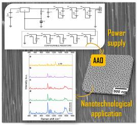
阳极材料由于其可定制的特性,为纳米技术的发展提供了一个通用的平台。我们的工作提出了一种成本效益高、用户友好的方法,通过硬阳极氧化(HA)制备高质量的阳极材料,这是应用最广泛的技术之一,通过施加高压在短时间内高效制备阳极氧化铝(AAO)平台。我们开发了一种具有简单拓扑结构的可配置电源,其最高可达190v,其管理由基本处理器板实现。此外,我们还实现了一个监测系统,用于获取过程阳极氧化参数。这种方法大大降低了传统方法(如电感式电源)的成本障碍。为了证明我们的战略实验装置的有效性,我们成功地制造了AAO模板,用作表面增强拉曼光谱(SERS)的衬底。因此,我们的低成本模块化友好实验装置为创建具有广泛应用于纳米技术的定义良好的纳米结构提供了一条有前途的途径。
本文章由计算机程序翻译,如有差异,请以英文原文为准。

Budget-friendly nanofabrication: Porous structures from high voltage DC and chemical etching

Budget-friendly nanofabrication: Porous structures from high voltage DC and chemical etching
Anodic materials provide a versatile platform for nanotechnological developments due to their customizable properties. Our work presents a cost-effective, user-friendly approach for fabricating high-quality anodic materials through hard anodization (HA), which is one of the most widely used techniques for efficiently fabricating anodic aluminum oxide (AAO) platforms in short times by applying high voltage. We developed a configurable power supply with a simple topology that can reach up to 190 V, which management was achieved by a basic processor board. In addition, we implemented a monitoring system for acquiring process anodization parameters. This approach significantly reduces the cost barrier associated with traditional methods, like induction-based power supplies. To demonstrate the effectiveness of our strategic experimental setup, we have successfully fabricated AAO templates to be used as substrates for surface-enhanced Raman spectroscopy (SERS). Thus, our low-cost modular friendly experimental setup offers a promising avenue for creating well-defined nanostructures with broad applications in nanotechnology.
求助全文
通过发布文献求助,成功后即可免费获取论文全文。 去求助
来源期刊
Current Applied Physics
Current Applied Physics 物理-材料科学:综合
CiteScore
4.80
自引率
0.00%
发文量
213
审稿时长
33 days
期刊介绍: Current Applied Physics (Curr. Appl. Phys.) is a monthly published international journal covering all the fields of applied science investigating the physics of the advanced materials for future applications. Other areas covered: Experimental and theoretical aspects of advanced materials and devices dealing with synthesis or structural chemistry, physical and electronic properties, photonics, engineering applications, and uniquely pertinent measurement or analytical techniques. Current Applied Physics, published since 2001, covers physics, chemistry and materials science, including bio-materials, with their engineering aspects. It is a truly interdisciplinary journal opening a forum for scientists of all related fields, a unique point of the journal discriminating it from other worldwide and/or Pacific Rim applied physics journals. Regular research papers, letters and review articles with contents meeting the scope of the journal will be considered for publication after peer review. The Journal is owned by the Korean Physical Society.
×
引用
GB/T 7714-2015
复制
MLA
复制
APA
复制
导出至
BibTeX EndNote RefMan NoteFirst NoteExpress
×
提示
您的信息不完整,为了账户安全,请先补充。
现在去补充
×
提示
您因"违规操作"
具体请查看互助需知
我知道了
×
提示
确定
请完成安全验证×
copy
已复制链接
快去分享给好友吧!
我知道了
右上角分享
点击右上角分享
0
联系我们:info@booksci.cn Book学术提供免费学术资源搜索服务,方便国内外学者检索中英文文献。致力于提供最便捷和优质的服务体验。 Copyright © 2023 布克学术 All rights reserved.
京ICP备2023020795号-1
ghs 京公网安备 11010802042870号
Book学术文献互助
Book学术文献互助群
群 号:604180095
Book学术官方微信