厚度可调的晶圆级单晶六方氮化硼的液态铜制备策略
IF 22
1区 材料科学
Q1 MATERIALS SCIENCE, MULTIDISCIPLINARY
引用次数: 0
摘要
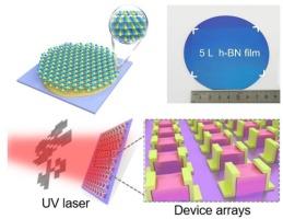
晶圆级单晶六方氮化硼(h-BN)薄膜可以作为一种优良的界面介电介质,是电子器件的理想平台。然而,这些实际应用需要大面积可控地合成单晶h-BN多层膜。在这里,我们展示了一种晶圆尺度的生长方法,可以实现精确的厚度可调的单晶h-BN多层膜,使用液态铜作为催化衬底。透射电子显微镜(TEM)和厘米级低能电子衍射(LEED)表征技术清楚地证明了晶圆级厚度可调的单晶h-BN多层膜的生产。所有证据表明,h-BN薄膜是通过圆形晶粒的自准直结合随后形成的圆形h-BN畴的过程产生的,可以进一步成核,生长并最终在先前形成的h-BN层表面合并成新的单晶层。这种液态金属方法为直接生长晶圆级单晶提供了一种可行的方法,为二维器件的广泛应用和其他vdW材料的合成提供了便利。本文章由计算机程序翻译,如有差异,请以英文原文为准。
A liquid copper strategy for wafer-scale single-crystalline hexagonal boron nitride with tunable thickness
Wafer-scale single-crystalline hexagonal boron nitride (h-BN) films can act as an excellent interface dielectric, and are highly desirable as an ideal platform for electronic devices. However, those practical applications require the controllable synthesis of single-crystalline h-BN multilayers over large area. Here, we demonstrate a wafer-scale growth approach that can realize precise thickness-tunable single-crystalline h-BN multilayer by using liquid copper as the catalytic substrate. The production of wafer-scale thickness-tunable single-crystalline h-BN multilayer is clearly evidenced by Transmission Electron Microscopy (TEM) and centimetre-scale characterization techniques of Low Energy Electron Diffraction (LEED). All evidences show that the h-BN films are produced via a self-collimation of circular grains combined with the process that subsequently created circular h-BN domains can be further nucleated, grown and finally coalesced into a new single crystalline layer on the surface of the previously formed h-BN layer. This liquid metal approach provides a feasible way to grow wafer-scale single-crystal directly, which facilitate the wide application of two-dimensional (2D) devices and synthesize of other vdW materials.
求助全文
通过发布文献求助,成功后即可免费获取论文全文。
去求助
来源期刊
Materials Today
工程技术-材料科学:综合
CiteScore
36.30
自引率
1.20%
发文量
237
审稿时长
23 days
期刊介绍:
Materials Today is the leading journal in the Materials Today family, focusing on the latest and most impactful work in the materials science community. With a reputation for excellence in news and reviews, the journal has now expanded its coverage to include original research and aims to be at the forefront of the field.
We welcome comprehensive articles, short communications, and review articles from established leaders in the rapidly evolving fields of materials science and related disciplines. We strive to provide authors with rigorous peer review, fast publication, and maximum exposure for their work. While we only accept the most significant manuscripts, our speedy evaluation process ensures that there are no unnecessary publication delays.
 求助内容:
求助内容: 应助结果提醒方式:


