Pinyi Wang, Siyuan Wang, Hailun Tang, Jing Ding, Xinyu Fang, Yang Yang, Xiao Huang* and Hai Li*,
{"title":"以十二烷基硫酸钠作为光探测器件种子促进剂的MoS2纳米螺旋的可控生长","authors":"Pinyi Wang, Siyuan Wang, Hailun Tang, Jing Ding, Xinyu Fang, Yang Yang, Xiao Huang* and Hai Li*, ","doi":"10.1021/acsanm.5c02928","DOIUrl":null,"url":null,"abstract":"<p >Due to their unique spiral structure, transition metal dichalcogenide (TMDC) nanospirals have shown unique electronic and optical properties and have been widely explored in the fields of hydrogen evolution reaction, optoelectronics, and nonlinear optics. Many TMDC nanospirals have been successfully synthesized by using the chemical vapor deposition (CVD) method. The precursor ratio and growth temperature were well regulated to grow various nanospirals. However, the influence of the concentration of the seeding promoter on growing TMDC nanospirals is unexplored. In this work, we use sodium dodecyl sulfate (SDS) as the seeding promoter to grow MoS<sub>2</sub> in the CVD process. MoS<sub>2</sub> nanosheets were controllably grown by using SDS with a high concentration, while MoS<sub>2</sub> nanospirals were obtained when SDS with a low concentration was used. Optical microscopy and atomic force microscopy (AFM) measurements showed that the MoS<sub>2</sub> nanospirals were uniformly distributed on small-sized monolayer MoS<sub>2</sub> nanosheets. The twist angle between the bottom MoS<sub>2</sub> spiral layer and monolayer nanosheet and the Moiré patterns were revealed by high-resolution transmission electron microscopy. The MoS<sub>2</sub> nanospiral-based device exhibits better optoelectronic performance than a nanosheet-based device, including carrier mobility, photoresponsivity, photosensitivity, and response time. Photoconductive AFM measurement shows that the photocurrent of the nanospiral is higher than that of the nanosheet. The excellent optoelectronic performance of MoS<sub>2</sub> nanospirals could be ascribed to the vertical conductivity, superior dielectric screening, and strain in the spiral step, which arise from the unique spiral structure. Our work indicates that the MoS<sub>2</sub> nanospiral could be used for the high-performance optoelectronic device.</p>","PeriodicalId":6,"journal":{"name":"ACS Applied Nano Materials","volume":"8 32","pages":"16134–16147"},"PeriodicalIF":5.5000,"publicationDate":"2025-08-02","publicationTypes":"Journal Article","fieldsOfStudy":null,"isOpenAccess":false,"openAccessPdf":"","citationCount":"0","resultStr":"{\"title\":\"Controllable Growth of MoS2 Nanospirals by Using Sodium Dodecyl Sulfate as a Seeding Promoter for Photodetection Devices\",\"authors\":\"Pinyi Wang, Siyuan Wang, Hailun Tang, Jing Ding, Xinyu Fang, Yang Yang, Xiao Huang* and Hai Li*, \",\"doi\":\"10.1021/acsanm.5c02928\",\"DOIUrl\":null,\"url\":null,\"abstract\":\"<p >Due to their unique spiral structure, transition metal dichalcogenide (TMDC) nanospirals have shown unique electronic and optical properties and have been widely explored in the fields of hydrogen evolution reaction, optoelectronics, and nonlinear optics. Many TMDC nanospirals have been successfully synthesized by using the chemical vapor deposition (CVD) method. The precursor ratio and growth temperature were well regulated to grow various nanospirals. However, the influence of the concentration of the seeding promoter on growing TMDC nanospirals is unexplored. In this work, we use sodium dodecyl sulfate (SDS) as the seeding promoter to grow MoS<sub>2</sub> in the CVD process. MoS<sub>2</sub> nanosheets were controllably grown by using SDS with a high concentration, while MoS<sub>2</sub> nanospirals were obtained when SDS with a low concentration was used. Optical microscopy and atomic force microscopy (AFM) measurements showed that the MoS<sub>2</sub> nanospirals were uniformly distributed on small-sized monolayer MoS<sub>2</sub> nanosheets. The twist angle between the bottom MoS<sub>2</sub> spiral layer and monolayer nanosheet and the Moiré patterns were revealed by high-resolution transmission electron microscopy. The MoS<sub>2</sub> nanospiral-based device exhibits better optoelectronic performance than a nanosheet-based device, including carrier mobility, photoresponsivity, photosensitivity, and response time. Photoconductive AFM measurement shows that the photocurrent of the nanospiral is higher than that of the nanosheet. The excellent optoelectronic performance of MoS<sub>2</sub> nanospirals could be ascribed to the vertical conductivity, superior dielectric screening, and strain in the spiral step, which arise from the unique spiral structure. Our work indicates that the MoS<sub>2</sub> nanospiral could be used for the high-performance optoelectronic device.</p>\",\"PeriodicalId\":6,\"journal\":{\"name\":\"ACS Applied Nano Materials\",\"volume\":\"8 32\",\"pages\":\"16134–16147\"},\"PeriodicalIF\":5.5000,\"publicationDate\":\"2025-08-02\",\"publicationTypes\":\"Journal Article\",\"fieldsOfStudy\":null,\"isOpenAccess\":false,\"openAccessPdf\":\"\",\"citationCount\":\"0\",\"resultStr\":null,\"platform\":\"Semanticscholar\",\"paperid\":null,\"PeriodicalName\":\"ACS Applied Nano Materials\",\"FirstCategoryId\":\"88\",\"ListUrlMain\":\"https://pubs.acs.org/doi/10.1021/acsanm.5c02928\",\"RegionNum\":2,\"RegionCategory\":\"材料科学\",\"ArticlePicture\":[],\"TitleCN\":null,\"AbstractTextCN\":null,\"PMCID\":null,\"EPubDate\":\"\",\"PubModel\":\"\",\"JCR\":\"Q2\",\"JCRName\":\"MATERIALS SCIENCE, MULTIDISCIPLINARY\",\"Score\":null,\"Total\":0}","platform":"Semanticscholar","paperid":null,"PeriodicalName":"ACS Applied Nano Materials","FirstCategoryId":"88","ListUrlMain":"https://pubs.acs.org/doi/10.1021/acsanm.5c02928","RegionNum":2,"RegionCategory":"材料科学","ArticlePicture":[],"TitleCN":null,"AbstractTextCN":null,"PMCID":null,"EPubDate":"","PubModel":"","JCR":"Q2","JCRName":"MATERIALS SCIENCE, MULTIDISCIPLINARY","Score":null,"Total":0}
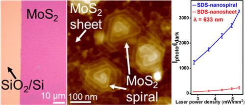
Controllable Growth of MoS2 Nanospirals by Using Sodium Dodecyl Sulfate as a Seeding Promoter for Photodetection Devices
Due to their unique spiral structure, transition metal dichalcogenide (TMDC) nanospirals have shown unique electronic and optical properties and have been widely explored in the fields of hydrogen evolution reaction, optoelectronics, and nonlinear optics. Many TMDC nanospirals have been successfully synthesized by using the chemical vapor deposition (CVD) method. The precursor ratio and growth temperature were well regulated to grow various nanospirals. However, the influence of the concentration of the seeding promoter on growing TMDC nanospirals is unexplored. In this work, we use sodium dodecyl sulfate (SDS) as the seeding promoter to grow MoS2 in the CVD process. MoS2 nanosheets were controllably grown by using SDS with a high concentration, while MoS2 nanospirals were obtained when SDS with a low concentration was used. Optical microscopy and atomic force microscopy (AFM) measurements showed that the MoS2 nanospirals were uniformly distributed on small-sized monolayer MoS2 nanosheets. The twist angle between the bottom MoS2 spiral layer and monolayer nanosheet and the Moiré patterns were revealed by high-resolution transmission electron microscopy. The MoS2 nanospiral-based device exhibits better optoelectronic performance than a nanosheet-based device, including carrier mobility, photoresponsivity, photosensitivity, and response time. Photoconductive AFM measurement shows that the photocurrent of the nanospiral is higher than that of the nanosheet. The excellent optoelectronic performance of MoS2 nanospirals could be ascribed to the vertical conductivity, superior dielectric screening, and strain in the spiral step, which arise from the unique spiral structure. Our work indicates that the MoS2 nanospiral could be used for the high-performance optoelectronic device.
期刊介绍:
ACS Applied Nano Materials is an interdisciplinary journal publishing original research covering all aspects of engineering, chemistry, physics and biology relevant to applications of nanomaterials. The journal is devoted to reports of new and original experimental and theoretical research of an applied nature that integrate knowledge in the areas of materials, engineering, physics, bioscience, and chemistry into important applications of nanomaterials.

 求助内容:
求助内容: 应助结果提醒方式:


