Meng Wang, Fengren Cao, Linxing Meng, Min Wang, Liang Li
{"title":"光电阵列与任意不可展开结构的直接集成","authors":"Meng Wang, Fengren Cao, Linxing Meng, Min Wang, Liang Li","doi":"10.1038/s41563-025-02322-7","DOIUrl":null,"url":null,"abstract":"<p>The extension of optoelectronic devices from planar to non-developable structures has led to remarkable success in bionics, optical imaging and soft electronics. However, non-developable optoelectronic devices are achieved mainly via physical deformations and limited to a few geometries. Here we report a self-assembly perovskite strategy for integrating optoelectronic arrays with arbitrary non-developable structures. The perovskite films are grown from a rapid nucleation-dominated crystallization driven by the low energy fluctuation of lead iodide solution, where the fluid precursor can be evenly dispersed along non-developable substrates by surface tension and then self-assembles into compact films through gaseous manipulation. The strategy covers arbitrarily shaped substrates with three-dimensional length scales over 10<sup>6</sup> orders of magnitude and enables the unique structural manipulations of photodiode arrays with micrometre precision. As a proof of concept, the theoretical focal surface of a single-lens image system is realized into a non-developable sensor, effectively correcting the off-axis coma aberrations compared with its planar or hemispherical counterpart.</p>","PeriodicalId":19058,"journal":{"name":"Nature Materials","volume":"105 1","pages":""},"PeriodicalIF":38.5000,"publicationDate":"2025-08-14","publicationTypes":"Journal Article","fieldsOfStudy":null,"isOpenAccess":false,"openAccessPdf":"","citationCount":"0","resultStr":"{\"title\":\"Direct integration of optoelectronic arrays with arbitrary non-developable structures\",\"authors\":\"Meng Wang, Fengren Cao, Linxing Meng, Min Wang, Liang Li\",\"doi\":\"10.1038/s41563-025-02322-7\",\"DOIUrl\":null,\"url\":null,\"abstract\":\"<p>The extension of optoelectronic devices from planar to non-developable structures has led to remarkable success in bionics, optical imaging and soft electronics. However, non-developable optoelectronic devices are achieved mainly via physical deformations and limited to a few geometries. Here we report a self-assembly perovskite strategy for integrating optoelectronic arrays with arbitrary non-developable structures. The perovskite films are grown from a rapid nucleation-dominated crystallization driven by the low energy fluctuation of lead iodide solution, where the fluid precursor can be evenly dispersed along non-developable substrates by surface tension and then self-assembles into compact films through gaseous manipulation. The strategy covers arbitrarily shaped substrates with three-dimensional length scales over 10<sup>6</sup> orders of magnitude and enables the unique structural manipulations of photodiode arrays with micrometre precision. As a proof of concept, the theoretical focal surface of a single-lens image system is realized into a non-developable sensor, effectively correcting the off-axis coma aberrations compared with its planar or hemispherical counterpart.</p>\",\"PeriodicalId\":19058,\"journal\":{\"name\":\"Nature Materials\",\"volume\":\"105 1\",\"pages\":\"\"},\"PeriodicalIF\":38.5000,\"publicationDate\":\"2025-08-14\",\"publicationTypes\":\"Journal Article\",\"fieldsOfStudy\":null,\"isOpenAccess\":false,\"openAccessPdf\":\"\",\"citationCount\":\"0\",\"resultStr\":null,\"platform\":\"Semanticscholar\",\"paperid\":null,\"PeriodicalName\":\"Nature Materials\",\"FirstCategoryId\":\"88\",\"ListUrlMain\":\"https://doi.org/10.1038/s41563-025-02322-7\",\"RegionNum\":1,\"RegionCategory\":\"材料科学\",\"ArticlePicture\":[],\"TitleCN\":null,\"AbstractTextCN\":null,\"PMCID\":null,\"EPubDate\":\"\",\"PubModel\":\"\",\"JCR\":\"Q1\",\"JCRName\":\"CHEMISTRY, PHYSICAL\",\"Score\":null,\"Total\":0}","platform":"Semanticscholar","paperid":null,"PeriodicalName":"Nature Materials","FirstCategoryId":"88","ListUrlMain":"https://doi.org/10.1038/s41563-025-02322-7","RegionNum":1,"RegionCategory":"材料科学","ArticlePicture":[],"TitleCN":null,"AbstractTextCN":null,"PMCID":null,"EPubDate":"","PubModel":"","JCR":"Q1","JCRName":"CHEMISTRY, PHYSICAL","Score":null,"Total":0}
Direct integration of optoelectronic arrays with arbitrary non-developable structures
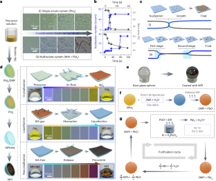
The extension of optoelectronic devices from planar to non-developable structures has led to remarkable success in bionics, optical imaging and soft electronics. However, non-developable optoelectronic devices are achieved mainly via physical deformations and limited to a few geometries. Here we report a self-assembly perovskite strategy for integrating optoelectronic arrays with arbitrary non-developable structures. The perovskite films are grown from a rapid nucleation-dominated crystallization driven by the low energy fluctuation of lead iodide solution, where the fluid precursor can be evenly dispersed along non-developable substrates by surface tension and then self-assembles into compact films through gaseous manipulation. The strategy covers arbitrarily shaped substrates with three-dimensional length scales over 106 orders of magnitude and enables the unique structural manipulations of photodiode arrays with micrometre precision. As a proof of concept, the theoretical focal surface of a single-lens image system is realized into a non-developable sensor, effectively correcting the off-axis coma aberrations compared with its planar or hemispherical counterpart.
期刊介绍:
Nature Materials is a monthly multi-disciplinary journal aimed at bringing together cutting-edge research across the entire spectrum of materials science and engineering. It covers all applied and fundamental aspects of the synthesis/processing, structure/composition, properties, and performance of materials. The journal recognizes that materials research has an increasing impact on classical disciplines such as physics, chemistry, and biology.
Additionally, Nature Materials provides a forum for the development of a common identity among materials scientists and encourages interdisciplinary collaboration. It takes an integrated and balanced approach to all areas of materials research, fostering the exchange of ideas between scientists involved in different disciplines.
Nature Materials is an invaluable resource for scientists in academia and industry who are active in discovering and developing materials and materials-related concepts. It offers engaging and informative papers of exceptional significance and quality, with the aim of influencing the development of society in the future.
 求助内容:
求助内容: 应助结果提醒方式:


