{"title":"考虑非均匀杂质颗粒分布的晶圆直接键合的数值和力学分析。","authors":"Feixiang Tang, Siyu He, Yuhan Li, Wenjin Liu, Fang Dong, Sheng Liu","doi":"10.1038/s41378-025-00994-4","DOIUrl":null,"url":null,"abstract":"<p><p>Direct wafer bonding allows polished semiconductor wafers to be joined together without the use of a binder. It has a wide range of applications in integrated circuit fabrication, micro-electro-mechanical systems (MEMS) packaging and multifunctional chip integration. Chip deflection and strain energy can be used to assess the bonding quality, and impurities have an important effect on the bonding quality. In this paper, a mathematical model and a finite element model of wafer bonding are established. The effects of different impurity distributions (Cluster, Complex, Face, Line) on the bonding quality of wafers are investigated, and the results show that the curvature and thickness of the wafer as well as the distribution of the impurity particles jointly determine the strain energy of the wafer under a certain pressure. Among them, the impurity particle surface distribution has the greatest influence on the wafer bonding quality. Finite element simulations verified the correctness of the proposed model. This work provides a theoretical basis for studying the effect of impurity distribution on wafer bonding performance.</p>","PeriodicalId":18560,"journal":{"name":"Microsystems & Nanoengineering","volume":"11 1","pages":"151"},"PeriodicalIF":9.9000,"publicationDate":"2025-08-12","publicationTypes":"Journal Article","fieldsOfStudy":null,"isOpenAccess":false,"openAccessPdf":"https://www.ncbi.nlm.nih.gov/pmc/articles/PMC12343963/pdf/","citationCount":"0","resultStr":"{\"title\":\"Numerical and Mechanical Analysis of Direct Wafer Bonding Considering Non-Uniform Impurity Particle Distributions.\",\"authors\":\"Feixiang Tang, Siyu He, Yuhan Li, Wenjin Liu, Fang Dong, Sheng Liu\",\"doi\":\"10.1038/s41378-025-00994-4\",\"DOIUrl\":null,\"url\":null,\"abstract\":\"<p><p>Direct wafer bonding allows polished semiconductor wafers to be joined together without the use of a binder. It has a wide range of applications in integrated circuit fabrication, micro-electro-mechanical systems (MEMS) packaging and multifunctional chip integration. Chip deflection and strain energy can be used to assess the bonding quality, and impurities have an important effect on the bonding quality. In this paper, a mathematical model and a finite element model of wafer bonding are established. The effects of different impurity distributions (Cluster, Complex, Face, Line) on the bonding quality of wafers are investigated, and the results show that the curvature and thickness of the wafer as well as the distribution of the impurity particles jointly determine the strain energy of the wafer under a certain pressure. Among them, the impurity particle surface distribution has the greatest influence on the wafer bonding quality. Finite element simulations verified the correctness of the proposed model. This work provides a theoretical basis for studying the effect of impurity distribution on wafer bonding performance.</p>\",\"PeriodicalId\":18560,\"journal\":{\"name\":\"Microsystems & Nanoengineering\",\"volume\":\"11 1\",\"pages\":\"151\"},\"PeriodicalIF\":9.9000,\"publicationDate\":\"2025-08-12\",\"publicationTypes\":\"Journal Article\",\"fieldsOfStudy\":null,\"isOpenAccess\":false,\"openAccessPdf\":\"https://www.ncbi.nlm.nih.gov/pmc/articles/PMC12343963/pdf/\",\"citationCount\":\"0\",\"resultStr\":null,\"platform\":\"Semanticscholar\",\"paperid\":null,\"PeriodicalName\":\"Microsystems & Nanoengineering\",\"FirstCategoryId\":\"5\",\"ListUrlMain\":\"https://doi.org/10.1038/s41378-025-00994-4\",\"RegionNum\":1,\"RegionCategory\":\"工程技术\",\"ArticlePicture\":[],\"TitleCN\":null,\"AbstractTextCN\":null,\"PMCID\":null,\"EPubDate\":\"\",\"PubModel\":\"\",\"JCR\":\"Q1\",\"JCRName\":\"INSTRUMENTS & INSTRUMENTATION\",\"Score\":null,\"Total\":0}","platform":"Semanticscholar","paperid":null,"PeriodicalName":"Microsystems & Nanoengineering","FirstCategoryId":"5","ListUrlMain":"https://doi.org/10.1038/s41378-025-00994-4","RegionNum":1,"RegionCategory":"工程技术","ArticlePicture":[],"TitleCN":null,"AbstractTextCN":null,"PMCID":null,"EPubDate":"","PubModel":"","JCR":"Q1","JCRName":"INSTRUMENTS & INSTRUMENTATION","Score":null,"Total":0}
Numerical and Mechanical Analysis of Direct Wafer Bonding Considering Non-Uniform Impurity Particle Distributions.
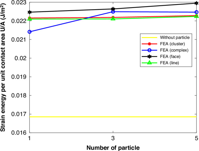
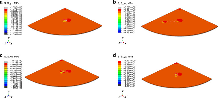
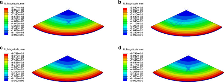
Direct wafer bonding allows polished semiconductor wafers to be joined together without the use of a binder. It has a wide range of applications in integrated circuit fabrication, micro-electro-mechanical systems (MEMS) packaging and multifunctional chip integration. Chip deflection and strain energy can be used to assess the bonding quality, and impurities have an important effect on the bonding quality. In this paper, a mathematical model and a finite element model of wafer bonding are established. The effects of different impurity distributions (Cluster, Complex, Face, Line) on the bonding quality of wafers are investigated, and the results show that the curvature and thickness of the wafer as well as the distribution of the impurity particles jointly determine the strain energy of the wafer under a certain pressure. Among them, the impurity particle surface distribution has the greatest influence on the wafer bonding quality. Finite element simulations verified the correctness of the proposed model. This work provides a theoretical basis for studying the effect of impurity distribution on wafer bonding performance.
期刊介绍:
Microsystems & Nanoengineering is a comprehensive online journal that focuses on the field of Micro and Nano Electro Mechanical Systems (MEMS and NEMS). It provides a platform for researchers to share their original research findings and review articles in this area. The journal covers a wide range of topics, from fundamental research to practical applications. Published by Springer Nature, in collaboration with the Aerospace Information Research Institute, Chinese Academy of Sciences, and with the support of the State Key Laboratory of Transducer Technology, it is an esteemed publication in the field. As an open access journal, it offers free access to its content, allowing readers from around the world to benefit from the latest developments in MEMS and NEMS.
 求助内容:
求助内容: 应助结果提醒方式:


