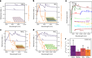
Panaiot G. Zotev, Paul Bouteyre, Yadong Wang, Sam A. Randerson, Xuerong Hu, Luca Sortino, Yue Wang, Timur Shegai, Su-Hyun Gong, Andreas Tittl, Igor Aharonovich, Alexander I. Tartakovskii
{"title":"多层范德华材料的纳米光子学","authors":"Panaiot G. Zotev, Paul Bouteyre, Yadong Wang, Sam A. Randerson, Xuerong Hu, Luca Sortino, Yue Wang, Timur Shegai, Su-Hyun Gong, Andreas Tittl, Igor Aharonovich, Alexander I. Tartakovskii","doi":"10.1038/s41566-025-01717-x","DOIUrl":null,"url":null,"abstract":"The field of nanophotonics requires high-quality materials for the fabrication of resonant structures that can confine light down to the nanoscale. Metallic nanostructures often used for this purpose exhibit high optical losses, so high-refractive-index dielectrics such as silicon (Si) and III–V semiconductors are widely used instead. Recently, layered materials, often referred to as ‘van der Waals materials’ for the forces holding atomic planes together in bulk crystals, have been introduced as alternative dielectric building blocks for nanophotonics. Compared to traditional semiconductors, these materials exhibit higher refractive indices and transparency in the visible and near-infrared favourable for compact waveguides; strong birefringence and large nonlinear optical coefficients attractive for nonlinear optics; and out-of-plane van der Waals adhesive forces enabling novel tuning techniques and heterointegration approaches for the realization of previously inaccessible photonic structures. Recently, these properties of quasi-bulk van der Waals materials (as opposed to their widely studied monolayers) have been applied in a variety of photonic structures and devices, which will be discussed here. We report on recent progress in utilizing layered materials in waveguiding, wavefront shaping, Purcell enhancement, quantum nanophotonics, lasing, nonlinear optics, and strong light–matter coupling, as well as offer a snapshot of future developments in hybrid and tunable nanophotonics, three-dimensional photonic structures, optical trapping, polariton devices and van der Waals integrated nanophotonic circuits. This Review reports the recent progress in utilizing van der Waals layered materials in various nanophotonics applications and provides an overview of their future developments in hybrid and tunable nanophotonics, 3D photonic structures, optical trapping, polariton devices and van der Waals integrated nanophotonic circuits.","PeriodicalId":18926,"journal":{"name":"Nature Photonics","volume":"19 8","pages":"788-802"},"PeriodicalIF":32.9000,"publicationDate":"2025-08-13","publicationTypes":"Journal Article","fieldsOfStudy":null,"isOpenAccess":false,"openAccessPdf":"","citationCount":"0","resultStr":"{\"title\":\"Nanophotonics with multilayer van der Waals materials\",\"authors\":\"Panaiot G. Zotev, Paul Bouteyre, Yadong Wang, Sam A. Randerson, Xuerong Hu, Luca Sortino, Yue Wang, Timur Shegai, Su-Hyun Gong, Andreas Tittl, Igor Aharonovich, Alexander I. Tartakovskii\",\"doi\":\"10.1038/s41566-025-01717-x\",\"DOIUrl\":null,\"url\":null,\"abstract\":\"The field of nanophotonics requires high-quality materials for the fabrication of resonant structures that can confine light down to the nanoscale. Metallic nanostructures often used for this purpose exhibit high optical losses, so high-refractive-index dielectrics such as silicon (Si) and III–V semiconductors are widely used instead. Recently, layered materials, often referred to as ‘van der Waals materials’ for the forces holding atomic planes together in bulk crystals, have been introduced as alternative dielectric building blocks for nanophotonics. Compared to traditional semiconductors, these materials exhibit higher refractive indices and transparency in the visible and near-infrared favourable for compact waveguides; strong birefringence and large nonlinear optical coefficients attractive for nonlinear optics; and out-of-plane van der Waals adhesive forces enabling novel tuning techniques and heterointegration approaches for the realization of previously inaccessible photonic structures. Recently, these properties of quasi-bulk van der Waals materials (as opposed to their widely studied monolayers) have been applied in a variety of photonic structures and devices, which will be discussed here. We report on recent progress in utilizing layered materials in waveguiding, wavefront shaping, Purcell enhancement, quantum nanophotonics, lasing, nonlinear optics, and strong light–matter coupling, as well as offer a snapshot of future developments in hybrid and tunable nanophotonics, three-dimensional photonic structures, optical trapping, polariton devices and van der Waals integrated nanophotonic circuits. This Review reports the recent progress in utilizing van der Waals layered materials in various nanophotonics applications and provides an overview of their future developments in hybrid and tunable nanophotonics, 3D photonic structures, optical trapping, polariton devices and van der Waals integrated nanophotonic circuits.\",\"PeriodicalId\":18926,\"journal\":{\"name\":\"Nature Photonics\",\"volume\":\"19 8\",\"pages\":\"788-802\"},\"PeriodicalIF\":32.9000,\"publicationDate\":\"2025-08-13\",\"publicationTypes\":\"Journal Article\",\"fieldsOfStudy\":null,\"isOpenAccess\":false,\"openAccessPdf\":\"\",\"citationCount\":\"0\",\"resultStr\":null,\"platform\":\"Semanticscholar\",\"paperid\":null,\"PeriodicalName\":\"Nature Photonics\",\"FirstCategoryId\":\"101\",\"ListUrlMain\":\"https://www.nature.com/articles/s41566-025-01717-x\",\"RegionNum\":1,\"RegionCategory\":\"物理与天体物理\",\"ArticlePicture\":[],\"TitleCN\":null,\"AbstractTextCN\":null,\"PMCID\":null,\"EPubDate\":\"\",\"PubModel\":\"\",\"JCR\":\"Q1\",\"JCRName\":\"OPTICS\",\"Score\":null,\"Total\":0}","platform":"Semanticscholar","paperid":null,"PeriodicalName":"Nature Photonics","FirstCategoryId":"101","ListUrlMain":"https://www.nature.com/articles/s41566-025-01717-x","RegionNum":1,"RegionCategory":"物理与天体物理","ArticlePicture":[],"TitleCN":null,"AbstractTextCN":null,"PMCID":null,"EPubDate":"","PubModel":"","JCR":"Q1","JCRName":"OPTICS","Score":null,"Total":0}
Nanophotonics with multilayer van der Waals materials
The field of nanophotonics requires high-quality materials for the fabrication of resonant structures that can confine light down to the nanoscale. Metallic nanostructures often used for this purpose exhibit high optical losses, so high-refractive-index dielectrics such as silicon (Si) and III–V semiconductors are widely used instead. Recently, layered materials, often referred to as ‘van der Waals materials’ for the forces holding atomic planes together in bulk crystals, have been introduced as alternative dielectric building blocks for nanophotonics. Compared to traditional semiconductors, these materials exhibit higher refractive indices and transparency in the visible and near-infrared favourable for compact waveguides; strong birefringence and large nonlinear optical coefficients attractive for nonlinear optics; and out-of-plane van der Waals adhesive forces enabling novel tuning techniques and heterointegration approaches for the realization of previously inaccessible photonic structures. Recently, these properties of quasi-bulk van der Waals materials (as opposed to their widely studied monolayers) have been applied in a variety of photonic structures and devices, which will be discussed here. We report on recent progress in utilizing layered materials in waveguiding, wavefront shaping, Purcell enhancement, quantum nanophotonics, lasing, nonlinear optics, and strong light–matter coupling, as well as offer a snapshot of future developments in hybrid and tunable nanophotonics, three-dimensional photonic structures, optical trapping, polariton devices and van der Waals integrated nanophotonic circuits. This Review reports the recent progress in utilizing van der Waals layered materials in various nanophotonics applications and provides an overview of their future developments in hybrid and tunable nanophotonics, 3D photonic structures, optical trapping, polariton devices and van der Waals integrated nanophotonic circuits.
期刊介绍:
Nature Photonics is a monthly journal dedicated to the scientific study and application of light, known as Photonics. It publishes top-quality, peer-reviewed research across all areas of light generation, manipulation, and detection.
The journal encompasses research into the fundamental properties of light and its interactions with matter, as well as the latest developments in optoelectronic devices and emerging photonics applications. Topics covered include lasers, LEDs, imaging, detectors, optoelectronic devices, quantum optics, biophotonics, optical data storage, spectroscopy, fiber optics, solar energy, displays, terahertz technology, nonlinear optics, plasmonics, nanophotonics, and X-rays.
In addition to research papers and review articles summarizing scientific findings in optoelectronics, Nature Photonics also features News and Views pieces and research highlights. It uniquely includes articles on the business aspects of the industry, such as technology commercialization and market analysis, offering a comprehensive perspective on the field.