{"title":"采用线性I-MOS变容管的130 nm CMOS交叉耦合宽带低相位噪声压控振荡器","authors":"Samad Jamali, Mehdi Ehsanian","doi":"10.1007/s10470-025-02472-3","DOIUrl":null,"url":null,"abstract":"<div><p>This paper presents a novel varactor-based voltage-controlled oscillator (VCO) designed in 130 nm CMOS technology, optimized for ultra-wide tuning range, low phase noise, and enhanced VCO gain (KVCO). The proposed architecture integrates two parallel inversion-mode MOS (I-MOS) transistors with fixed gate-to-drain capacitors. A single analog control voltage adjusts the effective capacitance, while a separate DC bias is applied to linearize the varactor’s response, improving KVCO linearity and tuning efficiency. Embedded within a cross-coupled VCO topology, the varactor provides tunable differential capacitance across the oscillator arms. The design achieves a tuning range of 88.3% (476 MHz to 1.23 GHz) and a phase noise of–153.7 dBc/Hz at 10 MHz offset. The resulting oscillator demonstrates a figure of merit (FoM) of 209.1 dBc/Hz and a tuning-aware FoM<sub>T</sub> of 228.6 dBc/Hz, making it suitable for low-power, wideband wireless communication applications.</p></div>","PeriodicalId":7827,"journal":{"name":"Analog Integrated Circuits and Signal Processing","volume":"124 3","pages":""},"PeriodicalIF":1.4000,"publicationDate":"2025-08-11","publicationTypes":"Journal Article","fieldsOfStudy":null,"isOpenAccess":false,"openAccessPdf":"","citationCount":"0","resultStr":"{\"title\":\"A cross-coupled wideband low-phase-noise VCO in 130 nm CMOS using a linear I-MOS varactor\",\"authors\":\"Samad Jamali, Mehdi Ehsanian\",\"doi\":\"10.1007/s10470-025-02472-3\",\"DOIUrl\":null,\"url\":null,\"abstract\":\"<div><p>This paper presents a novel varactor-based voltage-controlled oscillator (VCO) designed in 130 nm CMOS technology, optimized for ultra-wide tuning range, low phase noise, and enhanced VCO gain (KVCO). The proposed architecture integrates two parallel inversion-mode MOS (I-MOS) transistors with fixed gate-to-drain capacitors. A single analog control voltage adjusts the effective capacitance, while a separate DC bias is applied to linearize the varactor’s response, improving KVCO linearity and tuning efficiency. Embedded within a cross-coupled VCO topology, the varactor provides tunable differential capacitance across the oscillator arms. The design achieves a tuning range of 88.3% (476 MHz to 1.23 GHz) and a phase noise of–153.7 dBc/Hz at 10 MHz offset. The resulting oscillator demonstrates a figure of merit (FoM) of 209.1 dBc/Hz and a tuning-aware FoM<sub>T</sub> of 228.6 dBc/Hz, making it suitable for low-power, wideband wireless communication applications.</p></div>\",\"PeriodicalId\":7827,\"journal\":{\"name\":\"Analog Integrated Circuits and Signal Processing\",\"volume\":\"124 3\",\"pages\":\"\"},\"PeriodicalIF\":1.4000,\"publicationDate\":\"2025-08-11\",\"publicationTypes\":\"Journal Article\",\"fieldsOfStudy\":null,\"isOpenAccess\":false,\"openAccessPdf\":\"\",\"citationCount\":\"0\",\"resultStr\":null,\"platform\":\"Semanticscholar\",\"paperid\":null,\"PeriodicalName\":\"Analog Integrated Circuits and Signal Processing\",\"FirstCategoryId\":\"5\",\"ListUrlMain\":\"https://link.springer.com/article/10.1007/s10470-025-02472-3\",\"RegionNum\":4,\"RegionCategory\":\"工程技术\",\"ArticlePicture\":[],\"TitleCN\":null,\"AbstractTextCN\":null,\"PMCID\":null,\"EPubDate\":\"\",\"PubModel\":\"\",\"JCR\":\"Q4\",\"JCRName\":\"COMPUTER SCIENCE, HARDWARE & ARCHITECTURE\",\"Score\":null,\"Total\":0}","platform":"Semanticscholar","paperid":null,"PeriodicalName":"Analog Integrated Circuits and Signal Processing","FirstCategoryId":"5","ListUrlMain":"https://link.springer.com/article/10.1007/s10470-025-02472-3","RegionNum":4,"RegionCategory":"工程技术","ArticlePicture":[],"TitleCN":null,"AbstractTextCN":null,"PMCID":null,"EPubDate":"","PubModel":"","JCR":"Q4","JCRName":"COMPUTER SCIENCE, HARDWARE & ARCHITECTURE","Score":null,"Total":0}
A cross-coupled wideband low-phase-noise VCO in 130 nm CMOS using a linear I-MOS varactor
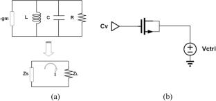
This paper presents a novel varactor-based voltage-controlled oscillator (VCO) designed in 130 nm CMOS technology, optimized for ultra-wide tuning range, low phase noise, and enhanced VCO gain (KVCO). The proposed architecture integrates two parallel inversion-mode MOS (I-MOS) transistors with fixed gate-to-drain capacitors. A single analog control voltage adjusts the effective capacitance, while a separate DC bias is applied to linearize the varactor’s response, improving KVCO linearity and tuning efficiency. Embedded within a cross-coupled VCO topology, the varactor provides tunable differential capacitance across the oscillator arms. The design achieves a tuning range of 88.3% (476 MHz to 1.23 GHz) and a phase noise of–153.7 dBc/Hz at 10 MHz offset. The resulting oscillator demonstrates a figure of merit (FoM) of 209.1 dBc/Hz and a tuning-aware FoMT of 228.6 dBc/Hz, making it suitable for low-power, wideband wireless communication applications.
期刊介绍:
Analog Integrated Circuits and Signal Processing is an archival peer reviewed journal dedicated to the design and application of analog, radio frequency (RF), and mixed signal integrated circuits (ICs) as well as signal processing circuits and systems. It features both new research results and tutorial views and reflects the large volume of cutting-edge research activity in the worldwide field today.
A partial list of topics includes analog and mixed signal interface circuits and systems; analog and RFIC design; data converters; active-RC, switched-capacitor, and continuous-time integrated filters; mixed analog/digital VLSI systems; wireless radio transceivers; clock and data recovery circuits; and high speed optoelectronic circuits and systems.


 求助内容:
求助内容: 应助结果提醒方式:


