{"title":"聚合物包裹单壁碳纳米管网络晶体管双极性输运的栅极介电效应","authors":"Walid Boukhili, Seung-Hoon Lee*, Quanhua Chen, Xiang Wan, Chee Leong Tan, Huabin Sun, Zhihao Yu, Yong Xu, Kang-Jun Baeg*, Beom-Goo Kang* and Dongyoon Khim*, ","doi":"10.1021/acsaelm.5c00747","DOIUrl":null,"url":null,"abstract":"<p >This study examines the effects of polymer gate dielectric layers on the charge transport properties of both holes and electrons in solution-processed polymer-wrapped single-walled carbon nanotube (s-SWCNT) network transistors. The dielectric constant plays a crucial role in determining charge transport characteristics, leading to a transition from hole-dominated to electron-dominated ambipolarity as it increases. To elucidate the underlying mechanisms, we analyze the contact resistance (<i>R</i><sub>c</sub>), effective trap state density (<i>N</i><sub>eff</sub>), and mobility in relation to the induced charge density (<i>Q</i><sub>ind</sub>). Our findings indicate that high-<i>k</i> polymer dielectrics exhibit two distinct effects: their randomly aligned dipoles induce energetic disorder at the s-SWCNT network interface, while their high capacitance reduces <i>R</i><sub>c</sub> and <i>N</i><sub>eff</sub>. Hole transport is primarily affected by energetic disorder, whereas electron transport is influenced by reduced <i>R</i><sub>c</sub> and <i>N</i><sub>eff</sub>. This difference arises due to variations in the Schottky–Mott limit between the gold source/drain electrodes and the conduction and valence bands.</p>","PeriodicalId":3,"journal":{"name":"ACS Applied Electronic Materials","volume":"7 13","pages":"6051–6061"},"PeriodicalIF":4.7000,"publicationDate":"2025-06-19","publicationTypes":"Journal Article","fieldsOfStudy":null,"isOpenAccess":false,"openAccessPdf":"","citationCount":"0","resultStr":"{\"title\":\"Gate Dielectric Effects on Ambipolar Transport in Polymer-Wrapped Single-Walled Carbon Nanotube Network Transistors\",\"authors\":\"Walid Boukhili, Seung-Hoon Lee*, Quanhua Chen, Xiang Wan, Chee Leong Tan, Huabin Sun, Zhihao Yu, Yong Xu, Kang-Jun Baeg*, Beom-Goo Kang* and Dongyoon Khim*, \",\"doi\":\"10.1021/acsaelm.5c00747\",\"DOIUrl\":null,\"url\":null,\"abstract\":\"<p >This study examines the effects of polymer gate dielectric layers on the charge transport properties of both holes and electrons in solution-processed polymer-wrapped single-walled carbon nanotube (s-SWCNT) network transistors. The dielectric constant plays a crucial role in determining charge transport characteristics, leading to a transition from hole-dominated to electron-dominated ambipolarity as it increases. To elucidate the underlying mechanisms, we analyze the contact resistance (<i>R</i><sub>c</sub>), effective trap state density (<i>N</i><sub>eff</sub>), and mobility in relation to the induced charge density (<i>Q</i><sub>ind</sub>). Our findings indicate that high-<i>k</i> polymer dielectrics exhibit two distinct effects: their randomly aligned dipoles induce energetic disorder at the s-SWCNT network interface, while their high capacitance reduces <i>R</i><sub>c</sub> and <i>N</i><sub>eff</sub>. Hole transport is primarily affected by energetic disorder, whereas electron transport is influenced by reduced <i>R</i><sub>c</sub> and <i>N</i><sub>eff</sub>. This difference arises due to variations in the Schottky–Mott limit between the gold source/drain electrodes and the conduction and valence bands.</p>\",\"PeriodicalId\":3,\"journal\":{\"name\":\"ACS Applied Electronic Materials\",\"volume\":\"7 13\",\"pages\":\"6051–6061\"},\"PeriodicalIF\":4.7000,\"publicationDate\":\"2025-06-19\",\"publicationTypes\":\"Journal Article\",\"fieldsOfStudy\":null,\"isOpenAccess\":false,\"openAccessPdf\":\"\",\"citationCount\":\"0\",\"resultStr\":null,\"platform\":\"Semanticscholar\",\"paperid\":null,\"PeriodicalName\":\"ACS Applied Electronic Materials\",\"FirstCategoryId\":\"88\",\"ListUrlMain\":\"https://pubs.acs.org/doi/10.1021/acsaelm.5c00747\",\"RegionNum\":3,\"RegionCategory\":\"材料科学\",\"ArticlePicture\":[],\"TitleCN\":null,\"AbstractTextCN\":null,\"PMCID\":null,\"EPubDate\":\"\",\"PubModel\":\"\",\"JCR\":\"Q1\",\"JCRName\":\"ENGINEERING, ELECTRICAL & ELECTRONIC\",\"Score\":null,\"Total\":0}","platform":"Semanticscholar","paperid":null,"PeriodicalName":"ACS Applied Electronic Materials","FirstCategoryId":"88","ListUrlMain":"https://pubs.acs.org/doi/10.1021/acsaelm.5c00747","RegionNum":3,"RegionCategory":"材料科学","ArticlePicture":[],"TitleCN":null,"AbstractTextCN":null,"PMCID":null,"EPubDate":"","PubModel":"","JCR":"Q1","JCRName":"ENGINEERING, ELECTRICAL & ELECTRONIC","Score":null,"Total":0}
Gate Dielectric Effects on Ambipolar Transport in Polymer-Wrapped Single-Walled Carbon Nanotube Network Transistors
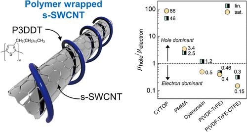
This study examines the effects of polymer gate dielectric layers on the charge transport properties of both holes and electrons in solution-processed polymer-wrapped single-walled carbon nanotube (s-SWCNT) network transistors. The dielectric constant plays a crucial role in determining charge transport characteristics, leading to a transition from hole-dominated to electron-dominated ambipolarity as it increases. To elucidate the underlying mechanisms, we analyze the contact resistance (Rc), effective trap state density (Neff), and mobility in relation to the induced charge density (Qind). Our findings indicate that high-k polymer dielectrics exhibit two distinct effects: their randomly aligned dipoles induce energetic disorder at the s-SWCNT network interface, while their high capacitance reduces Rc and Neff. Hole transport is primarily affected by energetic disorder, whereas electron transport is influenced by reduced Rc and Neff. This difference arises due to variations in the Schottky–Mott limit between the gold source/drain electrodes and the conduction and valence bands.
期刊介绍:
ACS Applied Electronic Materials is an interdisciplinary journal publishing original research covering all aspects of electronic materials. The journal is devoted to reports of new and original experimental and theoretical research of an applied nature that integrate knowledge in the areas of materials science, engineering, optics, physics, and chemistry into important applications of electronic materials. Sample research topics that span the journal's scope are inorganic, organic, ionic and polymeric materials with properties that include conducting, semiconducting, superconducting, insulating, dielectric, magnetic, optoelectronic, piezoelectric, ferroelectric and thermoelectric.
Indexed/Abstracted:
Web of Science SCIE
Scopus
CAS
INSPEC
Portico

 求助内容:
求助内容: 应助结果提醒方式:


