Ryoichiro Naoi, Durgadevi Elamaran and Daisuke Kiriya*,
{"title":"通过纳米厚的水溶性聚合物插入在二维材料中的接触工程","authors":"Ryoichiro Naoi, Durgadevi Elamaran and Daisuke Kiriya*, ","doi":"10.1021/acsaelm.5c00392","DOIUrl":null,"url":null,"abstract":"<p >In 2D layered materials, optimizing the metal contacts is a critical challenge for thin-film transistor applications. Transition metal dichalcogenides (TMDCs) are well-studied materials with atomic-level flatness, high mobility, and large electron mass, making them promising candidates to surpass silicon-based transistors. However, the Fermi level pinning (FLP) effect at the metal contact remains a key barrier. As of now, the insertion of 2D materials such as hexagonal boron nitride and deposited oxides has been demonstrated to reduce FLP, but these methods are neither scalable nor mild procedures near room temperature, which is necessary to avoid defect formation on TMDCs. Here, we demonstrate a solution-processable approach for forming a thin organic polymer layer (nm scale) on the contacts to suppress the FLP effect in WSe<sub>2</sub> transistors. The organic polymer used was poly-<span>l</span>-lysine (PLL) in an aqueous solution, and the key surface phenomenon is the spontaneous formation of a very thin polymer layer on the contacts through simple casting and rinsing during an intermediate treatment in the device fabrication process. The temperature-dependent transport characteristics and Schottky barrier height estimations of WSe<sub>2</sub> transistors demonstrate that inserting a PLL layer effectively reduces the FLP. The pinning factor (<i>S</i>) is significantly modulated from <i>S</i> = −0.001 in non-PLL-treated devices to −0.17 in PLL-treated devices, highlighting the effectiveness of PLL in mitigating FLP and improving interfacial energy alignment. This work uses a scalable solution process that relies simply on the interaction between the PLL polymer and the surface of WSe<sub>2</sub>. This approach offers a versatile strategy for improving device performance and can be extended to other 2D materials.</p>","PeriodicalId":3,"journal":{"name":"ACS Applied Electronic Materials","volume":"7 12","pages":"5418–5425"},"PeriodicalIF":4.7000,"publicationDate":"2025-06-12","publicationTypes":"Journal Article","fieldsOfStudy":null,"isOpenAccess":false,"openAccessPdf":"","citationCount":"0","resultStr":"{\"title\":\"Contact Engineering in 2D Materials via an nm -Thick Hydrosoluble Polymer Insertion\",\"authors\":\"Ryoichiro Naoi, Durgadevi Elamaran and Daisuke Kiriya*, \",\"doi\":\"10.1021/acsaelm.5c00392\",\"DOIUrl\":null,\"url\":null,\"abstract\":\"<p >In 2D layered materials, optimizing the metal contacts is a critical challenge for thin-film transistor applications. Transition metal dichalcogenides (TMDCs) are well-studied materials with atomic-level flatness, high mobility, and large electron mass, making them promising candidates to surpass silicon-based transistors. However, the Fermi level pinning (FLP) effect at the metal contact remains a key barrier. As of now, the insertion of 2D materials such as hexagonal boron nitride and deposited oxides has been demonstrated to reduce FLP, but these methods are neither scalable nor mild procedures near room temperature, which is necessary to avoid defect formation on TMDCs. Here, we demonstrate a solution-processable approach for forming a thin organic polymer layer (nm scale) on the contacts to suppress the FLP effect in WSe<sub>2</sub> transistors. The organic polymer used was poly-<span>l</span>-lysine (PLL) in an aqueous solution, and the key surface phenomenon is the spontaneous formation of a very thin polymer layer on the contacts through simple casting and rinsing during an intermediate treatment in the device fabrication process. The temperature-dependent transport characteristics and Schottky barrier height estimations of WSe<sub>2</sub> transistors demonstrate that inserting a PLL layer effectively reduces the FLP. The pinning factor (<i>S</i>) is significantly modulated from <i>S</i> = −0.001 in non-PLL-treated devices to −0.17 in PLL-treated devices, highlighting the effectiveness of PLL in mitigating FLP and improving interfacial energy alignment. This work uses a scalable solution process that relies simply on the interaction between the PLL polymer and the surface of WSe<sub>2</sub>. This approach offers a versatile strategy for improving device performance and can be extended to other 2D materials.</p>\",\"PeriodicalId\":3,\"journal\":{\"name\":\"ACS Applied Electronic Materials\",\"volume\":\"7 12\",\"pages\":\"5418–5425\"},\"PeriodicalIF\":4.7000,\"publicationDate\":\"2025-06-12\",\"publicationTypes\":\"Journal Article\",\"fieldsOfStudy\":null,\"isOpenAccess\":false,\"openAccessPdf\":\"\",\"citationCount\":\"0\",\"resultStr\":null,\"platform\":\"Semanticscholar\",\"paperid\":null,\"PeriodicalName\":\"ACS Applied Electronic Materials\",\"FirstCategoryId\":\"88\",\"ListUrlMain\":\"https://pubs.acs.org/doi/10.1021/acsaelm.5c00392\",\"RegionNum\":3,\"RegionCategory\":\"材料科学\",\"ArticlePicture\":[],\"TitleCN\":null,\"AbstractTextCN\":null,\"PMCID\":null,\"EPubDate\":\"\",\"PubModel\":\"\",\"JCR\":\"Q1\",\"JCRName\":\"ENGINEERING, ELECTRICAL & ELECTRONIC\",\"Score\":null,\"Total\":0}","platform":"Semanticscholar","paperid":null,"PeriodicalName":"ACS Applied Electronic Materials","FirstCategoryId":"88","ListUrlMain":"https://pubs.acs.org/doi/10.1021/acsaelm.5c00392","RegionNum":3,"RegionCategory":"材料科学","ArticlePicture":[],"TitleCN":null,"AbstractTextCN":null,"PMCID":null,"EPubDate":"","PubModel":"","JCR":"Q1","JCRName":"ENGINEERING, ELECTRICAL & ELECTRONIC","Score":null,"Total":0}
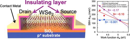
Contact Engineering in 2D Materials via an nm -Thick Hydrosoluble Polymer Insertion
In 2D layered materials, optimizing the metal contacts is a critical challenge for thin-film transistor applications. Transition metal dichalcogenides (TMDCs) are well-studied materials with atomic-level flatness, high mobility, and large electron mass, making them promising candidates to surpass silicon-based transistors. However, the Fermi level pinning (FLP) effect at the metal contact remains a key barrier. As of now, the insertion of 2D materials such as hexagonal boron nitride and deposited oxides has been demonstrated to reduce FLP, but these methods are neither scalable nor mild procedures near room temperature, which is necessary to avoid defect formation on TMDCs. Here, we demonstrate a solution-processable approach for forming a thin organic polymer layer (nm scale) on the contacts to suppress the FLP effect in WSe2 transistors. The organic polymer used was poly-l-lysine (PLL) in an aqueous solution, and the key surface phenomenon is the spontaneous formation of a very thin polymer layer on the contacts through simple casting and rinsing during an intermediate treatment in the device fabrication process. The temperature-dependent transport characteristics and Schottky barrier height estimations of WSe2 transistors demonstrate that inserting a PLL layer effectively reduces the FLP. The pinning factor (S) is significantly modulated from S = −0.001 in non-PLL-treated devices to −0.17 in PLL-treated devices, highlighting the effectiveness of PLL in mitigating FLP and improving interfacial energy alignment. This work uses a scalable solution process that relies simply on the interaction between the PLL polymer and the surface of WSe2. This approach offers a versatile strategy for improving device performance and can be extended to other 2D materials.
期刊介绍:
ACS Applied Electronic Materials is an interdisciplinary journal publishing original research covering all aspects of electronic materials. The journal is devoted to reports of new and original experimental and theoretical research of an applied nature that integrate knowledge in the areas of materials science, engineering, optics, physics, and chemistry into important applications of electronic materials. Sample research topics that span the journal's scope are inorganic, organic, ionic and polymeric materials with properties that include conducting, semiconducting, superconducting, insulating, dielectric, magnetic, optoelectronic, piezoelectric, ferroelectric and thermoelectric.
Indexed/Abstracted:
Web of Science SCIE
Scopus
CAS
INSPEC
Portico

 求助内容:
求助内容: 应助结果提醒方式:


