{"title":"用金属有机化学气相沉积技术在工业兼容的300毫米Si(100)衬底上制造940纳米微型发光二极管","authors":"Hadi Hijazi, Driss Mouloua, Mattéo Chobe, Léo Mallet-Dida, Mickael Martin, Jérémy Moeyaert, Sébastien Cavalaglio, Nathalia Massara, Juliette Mignot, Jérôme Richy, Philippe Grosse, Jean-Michel Hartmann, Thierry Baron","doi":"10.1002/adpr.202400226","DOIUrl":null,"url":null,"abstract":"<p>III-V light-emitting diodes (LEDs) have been attracting much interest due to their ability to cover a large spectrum of interesting wavelength for various applications. However, their incompatibility with integration on Si platforms compatible with complementary metal-oxide-semiconductor standards makes their high mass production a challenging task. Herein, the fabrication of 940 nm micro-LED on 300 mm Si wafers is reported. The active zone based on InGaAs/AlGaAs multiquantum wells is epitaxially grown by metal–organic chemical vapor deposition on two types of buffers, themselves on Si substrates: 500 nm thick GaAs and 500 nm GaAs 700 nm Ge bilayers. Very interesting results have been obtained on both structures in terms of external quantum efficiency (EQE), for example, about <span></span><math>\n <semantics>\n <mrow>\n <mn>2</mn>\n <mo> </mo>\n <mo>×</mo>\n <mo> </mo>\n <msup>\n <mrow>\n <mn>10</mn>\n </mrow>\n <mrow>\n <mo>−</mo>\n <mn>3</mn>\n </mrow>\n </msup>\n </mrow>\n <annotation>$2 \\textrm{ } \\times \\textrm{ } \\left(10\\right)^{- 3}$</annotation>\n </semantics></math>% and <span></span><math>\n <semantics>\n <mrow>\n <mn>0.4</mn>\n <mo> </mo>\n <mo>×</mo>\n <mo> </mo>\n <msup>\n <mrow>\n <mn>10</mn>\n </mrow>\n <mrow>\n <mo>−</mo>\n <mn>3</mn>\n </mrow>\n </msup>\n </mrow>\n <annotation>$0.4 \\textrm{ } \\times \\textrm{ } \\left(10\\right)^{- 3}$</annotation>\n </semantics></math>%, that is, 1/3rd and 1/15th the reference EQE obtained on bulk GaAs substrates. These results can easily be improved. Such demonstration offers a very promising roadmap for the monolithic integration of III-V μ-LED on Si platforms.</p>","PeriodicalId":7263,"journal":{"name":"Advanced Photonics Research","volume":"6 8","pages":""},"PeriodicalIF":3.9000,"publicationDate":"2025-04-25","publicationTypes":"Journal Article","fieldsOfStudy":null,"isOpenAccess":false,"openAccessPdf":"https://onlinelibrary.wiley.com/doi/epdf/10.1002/adpr.202400226","citationCount":"0","resultStr":"{\"title\":\"940 nm Micro-Light-Emitting Diode Fabricated on Industry-Compatible 300 mm Si (100) Substrate by Metal–Organic Chemical Vapor Deposition\",\"authors\":\"Hadi Hijazi, Driss Mouloua, Mattéo Chobe, Léo Mallet-Dida, Mickael Martin, Jérémy Moeyaert, Sébastien Cavalaglio, Nathalia Massara, Juliette Mignot, Jérôme Richy, Philippe Grosse, Jean-Michel Hartmann, Thierry Baron\",\"doi\":\"10.1002/adpr.202400226\",\"DOIUrl\":null,\"url\":null,\"abstract\":\"<p>III-V light-emitting diodes (LEDs) have been attracting much interest due to their ability to cover a large spectrum of interesting wavelength for various applications. However, their incompatibility with integration on Si platforms compatible with complementary metal-oxide-semiconductor standards makes their high mass production a challenging task. Herein, the fabrication of 940 nm micro-LED on 300 mm Si wafers is reported. The active zone based on InGaAs/AlGaAs multiquantum wells is epitaxially grown by metal–organic chemical vapor deposition on two types of buffers, themselves on Si substrates: 500 nm thick GaAs and 500 nm GaAs 700 nm Ge bilayers. Very interesting results have been obtained on both structures in terms of external quantum efficiency (EQE), for example, about <span></span><math>\\n <semantics>\\n <mrow>\\n <mn>2</mn>\\n <mo> </mo>\\n <mo>×</mo>\\n <mo> </mo>\\n <msup>\\n <mrow>\\n <mn>10</mn>\\n </mrow>\\n <mrow>\\n <mo>−</mo>\\n <mn>3</mn>\\n </mrow>\\n </msup>\\n </mrow>\\n <annotation>$2 \\\\textrm{ } \\\\times \\\\textrm{ } \\\\left(10\\\\right)^{- 3}$</annotation>\\n </semantics></math>% and <span></span><math>\\n <semantics>\\n <mrow>\\n <mn>0.4</mn>\\n <mo> </mo>\\n <mo>×</mo>\\n <mo> </mo>\\n <msup>\\n <mrow>\\n <mn>10</mn>\\n </mrow>\\n <mrow>\\n <mo>−</mo>\\n <mn>3</mn>\\n </mrow>\\n </msup>\\n </mrow>\\n <annotation>$0.4 \\\\textrm{ } \\\\times \\\\textrm{ } \\\\left(10\\\\right)^{- 3}$</annotation>\\n </semantics></math>%, that is, 1/3rd and 1/15th the reference EQE obtained on bulk GaAs substrates. These results can easily be improved. Such demonstration offers a very promising roadmap for the monolithic integration of III-V μ-LED on Si platforms.</p>\",\"PeriodicalId\":7263,\"journal\":{\"name\":\"Advanced Photonics Research\",\"volume\":\"6 8\",\"pages\":\"\"},\"PeriodicalIF\":3.9000,\"publicationDate\":\"2025-04-25\",\"publicationTypes\":\"Journal Article\",\"fieldsOfStudy\":null,\"isOpenAccess\":false,\"openAccessPdf\":\"https://onlinelibrary.wiley.com/doi/epdf/10.1002/adpr.202400226\",\"citationCount\":\"0\",\"resultStr\":null,\"platform\":\"Semanticscholar\",\"paperid\":null,\"PeriodicalName\":\"Advanced Photonics Research\",\"FirstCategoryId\":\"1085\",\"ListUrlMain\":\"https://advanced.onlinelibrary.wiley.com/doi/10.1002/adpr.202400226\",\"RegionNum\":0,\"RegionCategory\":null,\"ArticlePicture\":[],\"TitleCN\":null,\"AbstractTextCN\":null,\"PMCID\":null,\"EPubDate\":\"\",\"PubModel\":\"\",\"JCR\":\"Q2\",\"JCRName\":\"MATERIALS SCIENCE, MULTIDISCIPLINARY\",\"Score\":null,\"Total\":0}","platform":"Semanticscholar","paperid":null,"PeriodicalName":"Advanced Photonics Research","FirstCategoryId":"1085","ListUrlMain":"https://advanced.onlinelibrary.wiley.com/doi/10.1002/adpr.202400226","RegionNum":0,"RegionCategory":null,"ArticlePicture":[],"TitleCN":null,"AbstractTextCN":null,"PMCID":null,"EPubDate":"","PubModel":"","JCR":"Q2","JCRName":"MATERIALS SCIENCE, MULTIDISCIPLINARY","Score":null,"Total":0}
940 nm Micro-Light-Emitting Diode Fabricated on Industry-Compatible 300 mm Si (100) Substrate by Metal–Organic Chemical Vapor Deposition
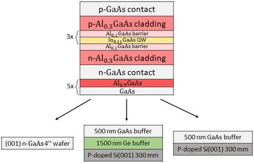
III-V light-emitting diodes (LEDs) have been attracting much interest due to their ability to cover a large spectrum of interesting wavelength for various applications. However, their incompatibility with integration on Si platforms compatible with complementary metal-oxide-semiconductor standards makes their high mass production a challenging task. Herein, the fabrication of 940 nm micro-LED on 300 mm Si wafers is reported. The active zone based on InGaAs/AlGaAs multiquantum wells is epitaxially grown by metal–organic chemical vapor deposition on two types of buffers, themselves on Si substrates: 500 nm thick GaAs and 500 nm GaAs 700 nm Ge bilayers. Very interesting results have been obtained on both structures in terms of external quantum efficiency (EQE), for example, about % and %, that is, 1/3rd and 1/15th the reference EQE obtained on bulk GaAs substrates. These results can easily be improved. Such demonstration offers a very promising roadmap for the monolithic integration of III-V μ-LED on Si platforms.


 求助内容:
求助内容: 应助结果提醒方式:


