Jing Xie, Ali Ebadi Yekta, Fahad Al Mamun, Kaichen Zhu, Maolin Chen, Sebastian Pazos, Wenwen Zheng, Xixiang Zhang, Seth Ariel Tongay, Xinyi Li, Huaqiang Wu, Robert Nemanich, Deji Akinwande, Mario Lanza, Ivan Sanchez Esqueda
{"title":"片上直接合成氮化硼忆阻器","authors":"Jing Xie, Ali Ebadi Yekta, Fahad Al Mamun, Kaichen Zhu, Maolin Chen, Sebastian Pazos, Wenwen Zheng, Xixiang Zhang, Seth Ariel Tongay, Xinyi Li, Huaqiang Wu, Robert Nemanich, Deji Akinwande, Mario Lanza, Ivan Sanchez Esqueda","doi":"10.1038/s41565-025-01988-z","DOIUrl":null,"url":null,"abstract":"<p>Two-dimensional materials hold promise for advanced complementary metal–oxide–semiconductor (CMOS) and beyond-CMOS electronics, including neuromorphic and in-memory computing. Hexagonal boron nitride (hBN) is particularly attractive for non-volatile resistive-switching devices (that is, memristors) due to its outstanding electronic, mechanical and chemical stability. However, integrating hBN memristors with Si-CMOS electronics faces challenges as it requires either high-temperature synthesis (exceeding thermal budgets) or transfer methods that introduce defects, impacting device performance and reliability. Here we introduce the synthesis of hBN films at CMOS-compatible temperatures (<380 °C) using electron cyclotron resonance plasma-enhanced chemical vapour deposition to realize transfer-free, CMOS-compatible hBN memristors with outstanding electrical characteristics. Our studies indicate a polycrystalline structure with turbostratic features in as-deposited hBN films and good wafer-level uniformity in morphology (size, shape and orientation). We demonstrate a large array of hBN memristors achieving high yield (~90%), stability (endurance, retention and repeatability), programming precision for multistate operation (>16 states) and low-frequency noise performance with minimal random telegraph noise. Furthermore, we directly integrate memristive devices on industrial CMOS test vehicles to demonstrate excellent endurance, achieving millions of programming cycles with a high technology readiness level. This represents an important step towards the wafer-scale CMOS integration of hBN-memristor-based electronics.</p>","PeriodicalId":18915,"journal":{"name":"Nature nanotechnology","volume":"216 1","pages":""},"PeriodicalIF":34.9000,"publicationDate":"2025-07-31","publicationTypes":"Journal Article","fieldsOfStudy":null,"isOpenAccess":false,"openAccessPdf":"","citationCount":"0","resultStr":"{\"title\":\"On-chip direct synthesis of boron nitride memristors\",\"authors\":\"Jing Xie, Ali Ebadi Yekta, Fahad Al Mamun, Kaichen Zhu, Maolin Chen, Sebastian Pazos, Wenwen Zheng, Xixiang Zhang, Seth Ariel Tongay, Xinyi Li, Huaqiang Wu, Robert Nemanich, Deji Akinwande, Mario Lanza, Ivan Sanchez Esqueda\",\"doi\":\"10.1038/s41565-025-01988-z\",\"DOIUrl\":null,\"url\":null,\"abstract\":\"<p>Two-dimensional materials hold promise for advanced complementary metal–oxide–semiconductor (CMOS) and beyond-CMOS electronics, including neuromorphic and in-memory computing. Hexagonal boron nitride (hBN) is particularly attractive for non-volatile resistive-switching devices (that is, memristors) due to its outstanding electronic, mechanical and chemical stability. However, integrating hBN memristors with Si-CMOS electronics faces challenges as it requires either high-temperature synthesis (exceeding thermal budgets) or transfer methods that introduce defects, impacting device performance and reliability. Here we introduce the synthesis of hBN films at CMOS-compatible temperatures (<380 °C) using electron cyclotron resonance plasma-enhanced chemical vapour deposition to realize transfer-free, CMOS-compatible hBN memristors with outstanding electrical characteristics. Our studies indicate a polycrystalline structure with turbostratic features in as-deposited hBN films and good wafer-level uniformity in morphology (size, shape and orientation). We demonstrate a large array of hBN memristors achieving high yield (~90%), stability (endurance, retention and repeatability), programming precision for multistate operation (>16 states) and low-frequency noise performance with minimal random telegraph noise. Furthermore, we directly integrate memristive devices on industrial CMOS test vehicles to demonstrate excellent endurance, achieving millions of programming cycles with a high technology readiness level. This represents an important step towards the wafer-scale CMOS integration of hBN-memristor-based electronics.</p>\",\"PeriodicalId\":18915,\"journal\":{\"name\":\"Nature nanotechnology\",\"volume\":\"216 1\",\"pages\":\"\"},\"PeriodicalIF\":34.9000,\"publicationDate\":\"2025-07-31\",\"publicationTypes\":\"Journal Article\",\"fieldsOfStudy\":null,\"isOpenAccess\":false,\"openAccessPdf\":\"\",\"citationCount\":\"0\",\"resultStr\":null,\"platform\":\"Semanticscholar\",\"paperid\":null,\"PeriodicalName\":\"Nature nanotechnology\",\"FirstCategoryId\":\"88\",\"ListUrlMain\":\"https://doi.org/10.1038/s41565-025-01988-z\",\"RegionNum\":1,\"RegionCategory\":\"材料科学\",\"ArticlePicture\":[],\"TitleCN\":null,\"AbstractTextCN\":null,\"PMCID\":null,\"EPubDate\":\"\",\"PubModel\":\"\",\"JCR\":\"Q1\",\"JCRName\":\"MATERIALS SCIENCE, MULTIDISCIPLINARY\",\"Score\":null,\"Total\":0}","platform":"Semanticscholar","paperid":null,"PeriodicalName":"Nature nanotechnology","FirstCategoryId":"88","ListUrlMain":"https://doi.org/10.1038/s41565-025-01988-z","RegionNum":1,"RegionCategory":"材料科学","ArticlePicture":[],"TitleCN":null,"AbstractTextCN":null,"PMCID":null,"EPubDate":"","PubModel":"","JCR":"Q1","JCRName":"MATERIALS SCIENCE, MULTIDISCIPLINARY","Score":null,"Total":0}
On-chip direct synthesis of boron nitride memristors
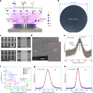
Two-dimensional materials hold promise for advanced complementary metal–oxide–semiconductor (CMOS) and beyond-CMOS electronics, including neuromorphic and in-memory computing. Hexagonal boron nitride (hBN) is particularly attractive for non-volatile resistive-switching devices (that is, memristors) due to its outstanding electronic, mechanical and chemical stability. However, integrating hBN memristors with Si-CMOS electronics faces challenges as it requires either high-temperature synthesis (exceeding thermal budgets) or transfer methods that introduce defects, impacting device performance and reliability. Here we introduce the synthesis of hBN films at CMOS-compatible temperatures (<380 °C) using electron cyclotron resonance plasma-enhanced chemical vapour deposition to realize transfer-free, CMOS-compatible hBN memristors with outstanding electrical characteristics. Our studies indicate a polycrystalline structure with turbostratic features in as-deposited hBN films and good wafer-level uniformity in morphology (size, shape and orientation). We demonstrate a large array of hBN memristors achieving high yield (~90%), stability (endurance, retention and repeatability), programming precision for multistate operation (>16 states) and low-frequency noise performance with minimal random telegraph noise. Furthermore, we directly integrate memristive devices on industrial CMOS test vehicles to demonstrate excellent endurance, achieving millions of programming cycles with a high technology readiness level. This represents an important step towards the wafer-scale CMOS integration of hBN-memristor-based electronics.
期刊介绍:
Nature Nanotechnology is a prestigious journal that publishes high-quality papers in various areas of nanoscience and nanotechnology. The journal focuses on the design, characterization, and production of structures, devices, and systems that manipulate and control materials at atomic, molecular, and macromolecular scales. It encompasses both bottom-up and top-down approaches, as well as their combinations.
Furthermore, Nature Nanotechnology fosters the exchange of ideas among researchers from diverse disciplines such as chemistry, physics, material science, biomedical research, engineering, and more. It promotes collaboration at the forefront of this multidisciplinary field. The journal covers a wide range of topics, from fundamental research in physics, chemistry, and biology, including computational work and simulations, to the development of innovative devices and technologies for various industrial sectors such as information technology, medicine, manufacturing, high-performance materials, energy, and environmental technologies. It includes coverage of organic, inorganic, and hybrid materials.
 求助内容:
求助内容: 应助结果提醒方式:


