{"title":"基于al介导催化剂工程的多周期GaAs/AlGaAs轴向异质结构纳米线晶体相位控制和室温随机激光。","authors":"Shan Wang, Bingheng Meng, Zhiyuan Ren, Yubin Kang, Jilong Tang, Xiaohua Wang*, Zhipeng Wei* and Rui Chen*, ","doi":"10.1021/acsami.5c12589","DOIUrl":null,"url":null,"abstract":"<p >Semiconductor axial heterostructure nanowires (NWs) offer unique advantages for nanophotonics but face challenges in achieving high crystal phase uniformity due to nucleation instability during growth, which limits their optoelectronic performance. In this study, Al-mediated catalyst engineering has been demonstrated to be an effective strategy for crystal phase control in multiperiod GaAs/Al<sub>0.4</sub>Ga<sub>0.6</sub>As axial heterostructure NWs fabricated by molecular beam epitaxy. By systematically varying the GaAs segment growth times (30, 60, 90, and 120 s), it was determined that all samples exhibit distinctive lotus-root morphology, and the 90 s sample (GaAs-90) achieves quasi-pure zincblende (ZB) phase formation. This is attributed to Al incorporation, reducing the Ga droplet size and liquid–vapor surface energy, thereby stabilizing ZB nucleation. Optical characterization reveals that GaAs-90 achieves room-temperature random lasing with a threshold of 55.59 mW/cm<sup>2</sup>. This study elucidates the critical synergy between crystal phase control and axial heterostructure design in achieving efficient NW random lasing, offering a scalable technological framework for on-chip integrated photonics.</p>","PeriodicalId":5,"journal":{"name":"ACS Applied Materials & Interfaces","volume":"17 31","pages":"45249–45257"},"PeriodicalIF":8.2000,"publicationDate":"2025-07-28","publicationTypes":"Journal Article","fieldsOfStudy":null,"isOpenAccess":false,"openAccessPdf":"","citationCount":"0","resultStr":"{\"title\":\"Crystal Phase Control and Room-Temperature Random Lasing in Multiperiod GaAs/AlGaAs Axial Heterostructure Nanowires via Al-Mediated Catalyst Engineering\",\"authors\":\"Shan Wang, Bingheng Meng, Zhiyuan Ren, Yubin Kang, Jilong Tang, Xiaohua Wang*, Zhipeng Wei* and Rui Chen*, \",\"doi\":\"10.1021/acsami.5c12589\",\"DOIUrl\":null,\"url\":null,\"abstract\":\"<p >Semiconductor axial heterostructure nanowires (NWs) offer unique advantages for nanophotonics but face challenges in achieving high crystal phase uniformity due to nucleation instability during growth, which limits their optoelectronic performance. In this study, Al-mediated catalyst engineering has been demonstrated to be an effective strategy for crystal phase control in multiperiod GaAs/Al<sub>0.4</sub>Ga<sub>0.6</sub>As axial heterostructure NWs fabricated by molecular beam epitaxy. By systematically varying the GaAs segment growth times (30, 60, 90, and 120 s), it was determined that all samples exhibit distinctive lotus-root morphology, and the 90 s sample (GaAs-90) achieves quasi-pure zincblende (ZB) phase formation. This is attributed to Al incorporation, reducing the Ga droplet size and liquid–vapor surface energy, thereby stabilizing ZB nucleation. Optical characterization reveals that GaAs-90 achieves room-temperature random lasing with a threshold of 55.59 mW/cm<sup>2</sup>. This study elucidates the critical synergy between crystal phase control and axial heterostructure design in achieving efficient NW random lasing, offering a scalable technological framework for on-chip integrated photonics.</p>\",\"PeriodicalId\":5,\"journal\":{\"name\":\"ACS Applied Materials & Interfaces\",\"volume\":\"17 31\",\"pages\":\"45249–45257\"},\"PeriodicalIF\":8.2000,\"publicationDate\":\"2025-07-28\",\"publicationTypes\":\"Journal Article\",\"fieldsOfStudy\":null,\"isOpenAccess\":false,\"openAccessPdf\":\"\",\"citationCount\":\"0\",\"resultStr\":null,\"platform\":\"Semanticscholar\",\"paperid\":null,\"PeriodicalName\":\"ACS Applied Materials & Interfaces\",\"FirstCategoryId\":\"88\",\"ListUrlMain\":\"https://pubs.acs.org/doi/10.1021/acsami.5c12589\",\"RegionNum\":2,\"RegionCategory\":\"材料科学\",\"ArticlePicture\":[],\"TitleCN\":null,\"AbstractTextCN\":null,\"PMCID\":null,\"EPubDate\":\"\",\"PubModel\":\"\",\"JCR\":\"Q1\",\"JCRName\":\"MATERIALS SCIENCE, MULTIDISCIPLINARY\",\"Score\":null,\"Total\":0}","platform":"Semanticscholar","paperid":null,"PeriodicalName":"ACS Applied Materials & Interfaces","FirstCategoryId":"88","ListUrlMain":"https://pubs.acs.org/doi/10.1021/acsami.5c12589","RegionNum":2,"RegionCategory":"材料科学","ArticlePicture":[],"TitleCN":null,"AbstractTextCN":null,"PMCID":null,"EPubDate":"","PubModel":"","JCR":"Q1","JCRName":"MATERIALS SCIENCE, MULTIDISCIPLINARY","Score":null,"Total":0}
Crystal Phase Control and Room-Temperature Random Lasing in Multiperiod GaAs/AlGaAs Axial Heterostructure Nanowires via Al-Mediated Catalyst Engineering
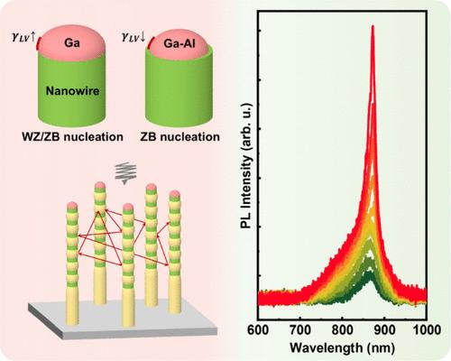
Semiconductor axial heterostructure nanowires (NWs) offer unique advantages for nanophotonics but face challenges in achieving high crystal phase uniformity due to nucleation instability during growth, which limits their optoelectronic performance. In this study, Al-mediated catalyst engineering has been demonstrated to be an effective strategy for crystal phase control in multiperiod GaAs/Al0.4Ga0.6As axial heterostructure NWs fabricated by molecular beam epitaxy. By systematically varying the GaAs segment growth times (30, 60, 90, and 120 s), it was determined that all samples exhibit distinctive lotus-root morphology, and the 90 s sample (GaAs-90) achieves quasi-pure zincblende (ZB) phase formation. This is attributed to Al incorporation, reducing the Ga droplet size and liquid–vapor surface energy, thereby stabilizing ZB nucleation. Optical characterization reveals that GaAs-90 achieves room-temperature random lasing with a threshold of 55.59 mW/cm2. This study elucidates the critical synergy between crystal phase control and axial heterostructure design in achieving efficient NW random lasing, offering a scalable technological framework for on-chip integrated photonics.
期刊介绍:
ACS Applied Materials & Interfaces is a leading interdisciplinary journal that brings together chemists, engineers, physicists, and biologists to explore the development and utilization of newly-discovered materials and interfacial processes for specific applications. Our journal has experienced remarkable growth since its establishment in 2009, both in terms of the number of articles published and the impact of the research showcased. We are proud to foster a truly global community, with the majority of published articles originating from outside the United States, reflecting the rapid growth of applied research worldwide.

 求助内容:
求助内容: 应助结果提醒方式:


