Anna Varini, Cyrille Masserey, Vanessa Conti, Zahra Saadat Somaehsofla, Ehsan Ansari, Igor Stolichnov and Adrian M. Ionescu*,
{"title":"脉冲激光和原子层沉积cmos兼容二氧化钒:实现超薄相变膜。","authors":"Anna Varini, Cyrille Masserey, Vanessa Conti, Zahra Saadat Somaehsofla, Ehsan Ansari, Igor Stolichnov and Adrian M. Ionescu*, ","doi":"10.1021/acsaelm.5c01132","DOIUrl":null,"url":null,"abstract":"<p >Vanadium dioxide (VO<sub>2</sub>), a well-known Mott insulator, is a highly studied electronic material with promising applications in information processing and storage, including neuromorphic and brain-inspired electronics, high-frequency reconfigurable electronics, optoelectronic modulators, sensors, and smart windows with thermal regulation. While epitaxial VO<sub>2</sub> layers exhibit exceptional properties, such as a sharp and abrupt conductivity change at the metal–insulator transition, fabricating polycrystalline VO<sub>2</sub> films on silicon substrates often involves trade-offs in transport characteristics and switching performance, especially for ultrathin layers required in advanced gate applications. In this study, we explore the growth dynamics of VO<sub>2</sub> films on standard CMOS-compatible wet-oxidized silicon wafers by using two established deposition techniques: pulsed laser deposition (PLD) and atomic layer deposition (ALD). VO<sub>2</sub> films, ranging in thickness from 200 nm to less than 10 nm, were systematically characterized through structural and electrical analyses to optimize key growth parameters. In this study, the temperature and pressure were identified as the key factors influencing the morphology and quality of switching in VO2 films. The growth dynamics and optimal growth conditions across the entire thickness range are discussed in detail. PLD and ALD offer distinct advantages: PLD enables the formation of high-density films, while ALD allows for conformal deposition on complex 3D structures. We demonstrate that both methods can successfully produce ultrathin VO<sub>2</sub> layers down to 6–8 nm with functional properties suitable for practical applications, provided that growth parameters are carefully optimized. This work underscores the potential of VO<sub>2</sub> for fully CMOS-compatible phase-change switching devices and provides valuable insights into optimizing growth processes for polycrystalline VO<sub>2</sub> films grown with different techniques, including widely used magnetron sputtering.</p>","PeriodicalId":3,"journal":{"name":"ACS Applied Electronic Materials","volume":"7 14","pages":"6707–6719"},"PeriodicalIF":4.7000,"publicationDate":"2025-07-02","publicationTypes":"Journal Article","fieldsOfStudy":null,"isOpenAccess":false,"openAccessPdf":"https://www.ncbi.nlm.nih.gov/pmc/articles/PMC12288059/pdf/","citationCount":"0","resultStr":"{\"title\":\"Pulsed Laser and Atomic Layer Deposition of CMOS-Compatible Vanadium Dioxide: Enabling Ultrathin Phase-Change Films\",\"authors\":\"Anna Varini, Cyrille Masserey, Vanessa Conti, Zahra Saadat Somaehsofla, Ehsan Ansari, Igor Stolichnov and Adrian M. Ionescu*, \",\"doi\":\"10.1021/acsaelm.5c01132\",\"DOIUrl\":null,\"url\":null,\"abstract\":\"<p >Vanadium dioxide (VO<sub>2</sub>), a well-known Mott insulator, is a highly studied electronic material with promising applications in information processing and storage, including neuromorphic and brain-inspired electronics, high-frequency reconfigurable electronics, optoelectronic modulators, sensors, and smart windows with thermal regulation. While epitaxial VO<sub>2</sub> layers exhibit exceptional properties, such as a sharp and abrupt conductivity change at the metal–insulator transition, fabricating polycrystalline VO<sub>2</sub> films on silicon substrates often involves trade-offs in transport characteristics and switching performance, especially for ultrathin layers required in advanced gate applications. In this study, we explore the growth dynamics of VO<sub>2</sub> films on standard CMOS-compatible wet-oxidized silicon wafers by using two established deposition techniques: pulsed laser deposition (PLD) and atomic layer deposition (ALD). VO<sub>2</sub> films, ranging in thickness from 200 nm to less than 10 nm, were systematically characterized through structural and electrical analyses to optimize key growth parameters. In this study, the temperature and pressure were identified as the key factors influencing the morphology and quality of switching in VO2 films. The growth dynamics and optimal growth conditions across the entire thickness range are discussed in detail. PLD and ALD offer distinct advantages: PLD enables the formation of high-density films, while ALD allows for conformal deposition on complex 3D structures. We demonstrate that both methods can successfully produce ultrathin VO<sub>2</sub> layers down to 6–8 nm with functional properties suitable for practical applications, provided that growth parameters are carefully optimized. This work underscores the potential of VO<sub>2</sub> for fully CMOS-compatible phase-change switching devices and provides valuable insights into optimizing growth processes for polycrystalline VO<sub>2</sub> films grown with different techniques, including widely used magnetron sputtering.</p>\",\"PeriodicalId\":3,\"journal\":{\"name\":\"ACS Applied Electronic Materials\",\"volume\":\"7 14\",\"pages\":\"6707–6719\"},\"PeriodicalIF\":4.7000,\"publicationDate\":\"2025-07-02\",\"publicationTypes\":\"Journal Article\",\"fieldsOfStudy\":null,\"isOpenAccess\":false,\"openAccessPdf\":\"https://www.ncbi.nlm.nih.gov/pmc/articles/PMC12288059/pdf/\",\"citationCount\":\"0\",\"resultStr\":null,\"platform\":\"Semanticscholar\",\"paperid\":null,\"PeriodicalName\":\"ACS Applied Electronic Materials\",\"FirstCategoryId\":\"88\",\"ListUrlMain\":\"https://pubs.acs.org/doi/10.1021/acsaelm.5c01132\",\"RegionNum\":3,\"RegionCategory\":\"材料科学\",\"ArticlePicture\":[],\"TitleCN\":null,\"AbstractTextCN\":null,\"PMCID\":null,\"EPubDate\":\"\",\"PubModel\":\"\",\"JCR\":\"Q1\",\"JCRName\":\"ENGINEERING, ELECTRICAL & ELECTRONIC\",\"Score\":null,\"Total\":0}","platform":"Semanticscholar","paperid":null,"PeriodicalName":"ACS Applied Electronic Materials","FirstCategoryId":"88","ListUrlMain":"https://pubs.acs.org/doi/10.1021/acsaelm.5c01132","RegionNum":3,"RegionCategory":"材料科学","ArticlePicture":[],"TitleCN":null,"AbstractTextCN":null,"PMCID":null,"EPubDate":"","PubModel":"","JCR":"Q1","JCRName":"ENGINEERING, ELECTRICAL & ELECTRONIC","Score":null,"Total":0}
Pulsed Laser and Atomic Layer Deposition of CMOS-Compatible Vanadium Dioxide: Enabling Ultrathin Phase-Change Films
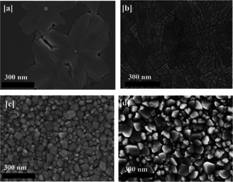
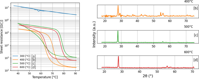
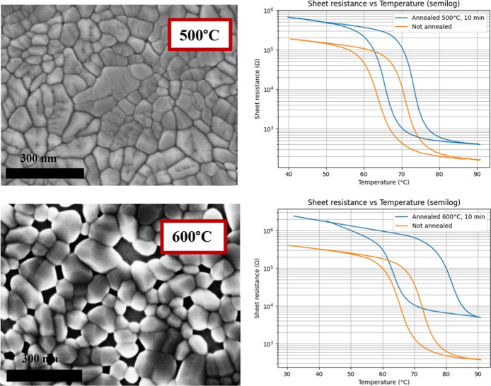
Vanadium dioxide (VO2), a well-known Mott insulator, is a highly studied electronic material with promising applications in information processing and storage, including neuromorphic and brain-inspired electronics, high-frequency reconfigurable electronics, optoelectronic modulators, sensors, and smart windows with thermal regulation. While epitaxial VO2 layers exhibit exceptional properties, such as a sharp and abrupt conductivity change at the metal–insulator transition, fabricating polycrystalline VO2 films on silicon substrates often involves trade-offs in transport characteristics and switching performance, especially for ultrathin layers required in advanced gate applications. In this study, we explore the growth dynamics of VO2 films on standard CMOS-compatible wet-oxidized silicon wafers by using two established deposition techniques: pulsed laser deposition (PLD) and atomic layer deposition (ALD). VO2 films, ranging in thickness from 200 nm to less than 10 nm, were systematically characterized through structural and electrical analyses to optimize key growth parameters. In this study, the temperature and pressure were identified as the key factors influencing the morphology and quality of switching in VO2 films. The growth dynamics and optimal growth conditions across the entire thickness range are discussed in detail. PLD and ALD offer distinct advantages: PLD enables the formation of high-density films, while ALD allows for conformal deposition on complex 3D structures. We demonstrate that both methods can successfully produce ultrathin VO2 layers down to 6–8 nm with functional properties suitable for practical applications, provided that growth parameters are carefully optimized. This work underscores the potential of VO2 for fully CMOS-compatible phase-change switching devices and provides valuable insights into optimizing growth processes for polycrystalline VO2 films grown with different techniques, including widely used magnetron sputtering.
期刊介绍:
ACS Applied Electronic Materials is an interdisciplinary journal publishing original research covering all aspects of electronic materials. The journal is devoted to reports of new and original experimental and theoretical research of an applied nature that integrate knowledge in the areas of materials science, engineering, optics, physics, and chemistry into important applications of electronic materials. Sample research topics that span the journal's scope are inorganic, organic, ionic and polymeric materials with properties that include conducting, semiconducting, superconducting, insulating, dielectric, magnetic, optoelectronic, piezoelectric, ferroelectric and thermoelectric.
Indexed/Abstracted:
Web of Science SCIE
Scopus
CAS
INSPEC
Portico

 求助内容:
求助内容: 应助结果提醒方式:


