用单层二硒化钨制备竞争性p通道
IF 40.9
1区 工程技术
Q1 ENGINEERING, ELECTRICAL & ELECTRONIC
引用次数: 0
摘要
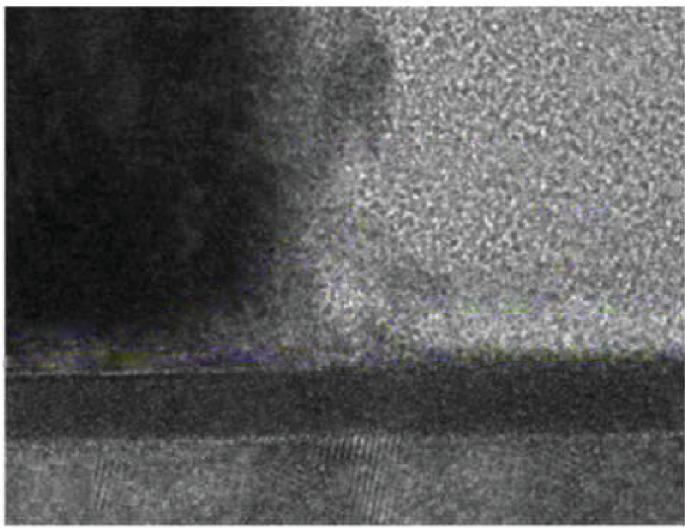
来自台湾半导体制造公司、国立台湾大学和国立阳明交通大学的研究人员开发了一种系统的方法来优化通道接口和提高晶体管性能。为了减轻由转移过程引起的可变性,对衬底进行预处理,使介电界面亲水,然后清洗以去除任何残留物。在WSe2表面涂上一层牺牲接触缓冲层以防止光刻引起的缺陷,并在WSe2和钯电极之间插入接触衬垫以减少费米能级钉钉(衬垫材料的详细信息未给出)。晶体管有一层4纳米厚的氧化铪(HfOx)作为电介质。经过自由基后处理和钝化处理后,器件在漏极电压为- 1 V时的导通电流为400 μA μm−1,亚阈值摆幅为72 mV / 10年,通/关比为107,迟滞最小。暴露在空气中一周后,它们也没有表现出性能下降。原始参考:具有单层WSe2通道的PMOS的性能提升。在Proc 2025 IEEE VLSI技术研讨会&;电路(2025);https://www.vlsisymposium.org/本文章由计算机程序翻译,如有差异,请以英文原文为准。
Making competitive p-channels from monolayer tungsten diselenide
求助全文
通过发布文献求助,成功后即可免费获取论文全文。
去求助
来源期刊
Nature Electronics
Engineering-Electrical and Electronic Engineering
CiteScore
47.50
自引率
2.30%
发文量
159
期刊介绍:
Nature Electronics is a comprehensive journal that publishes both fundamental and applied research in the field of electronics. It encompasses a wide range of topics, including the study of new phenomena and devices, the design and construction of electronic circuits, and the practical applications of electronics. In addition, the journal explores the commercial and industrial aspects of electronics research.
The primary focus of Nature Electronics is on the development of technology and its potential impact on society. The journal incorporates the contributions of scientists, engineers, and industry professionals, offering a platform for their research findings. Moreover, Nature Electronics provides insightful commentary, thorough reviews, and analysis of the key issues that shape the field, as well as the technologies that are reshaping society.
Like all journals within the prestigious Nature brand, Nature Electronics upholds the highest standards of quality. It maintains a dedicated team of professional editors and follows a fair and rigorous peer-review process. The journal also ensures impeccable copy-editing and production, enabling swift publication. Additionally, Nature Electronics prides itself on its editorial independence, ensuring unbiased and impartial reporting.
In summary, Nature Electronics is a leading journal that publishes cutting-edge research in electronics. With its multidisciplinary approach and commitment to excellence, the journal serves as a valuable resource for scientists, engineers, and industry professionals seeking to stay at the forefront of advancements in the field.
 求助内容:
求助内容: 应助结果提醒方式:


