栅极长度为10nm的间隔设计的GS SOI n-FinFET的性能增强

IF 3.1 4区 工程技术 Q2 ENGINEERING, ELECTRICAL & ELECTRONIC
Bhavya Kumar , Anurag Somayajula , Vishnu Sajith , Tanish Aggarwal , Rishu Chaujar
{"title":"栅极长度为10nm的间隔设计的GS SOI n-FinFET的性能增强","authors":"Bhavya Kumar ,&nbsp;Anurag Somayajula ,&nbsp;Vishnu Sajith ,&nbsp;Tanish Aggarwal ,&nbsp;Rishu Chaujar","doi":"10.1016/j.mee.2025.112383","DOIUrl":null,"url":null,"abstract":"<div><div>This study showcases the improvement in conventional SOI n-FinFET devices with the incorporation of a high-K spacer and gate stack (GS) engineering at 10 nm gate length. Three FinFET configurations were considered for comparison, and the simulated results show significant improvements in the analog and RF performance of the proposed configuration. Analog parameters such as the I<sub>ON</sub>/I<sub>OFF</sub> ratio increased almost 10<sup>4</sup> times, subthreshold swing reduced by ∼60 %; transconductance increased by ∼92 %, QF improved by ∼382 %, TGF enhanced by ∼302 %, intrinsic gain increased by almost 8 times, and early voltage by almost 5 times, indicating the proposed device is suitable for high-performance CMOS circuits. Further, the RF analysis is performed with parameters like cut-off frequency, GFP, TFP, etc., exhibiting considerable improvement for the proposed configuration. Thus, gate stacking and spacer engineering significantly improve the FinFET performance, enhancing the analog and RF capabilities of semiconductor devices for more efficient integrated circuits.</div></div>","PeriodicalId":18557,"journal":{"name":"Microelectronic Engineering","volume":"300 ","pages":"Article 112383"},"PeriodicalIF":3.1000,"publicationDate":"2025-07-16","publicationTypes":"Journal Article","fieldsOfStudy":null,"isOpenAccess":false,"openAccessPdf":"","citationCount":"0","resultStr":"{\"title\":\"Performance enhancement of a spacer-engineered GS SOI n-FinFET with 10 nm gate length\",\"authors\":\"Bhavya Kumar ,&nbsp;Anurag Somayajula ,&nbsp;Vishnu Sajith ,&nbsp;Tanish Aggarwal ,&nbsp;Rishu Chaujar\",\"doi\":\"10.1016/j.mee.2025.112383\",\"DOIUrl\":null,\"url\":null,\"abstract\":\"<div><div>This study showcases the improvement in conventional SOI n-FinFET devices with the incorporation of a high-K spacer and gate stack (GS) engineering at 10 nm gate length. Three FinFET configurations were considered for comparison, and the simulated results show significant improvements in the analog and RF performance of the proposed configuration. Analog parameters such as the I<sub>ON</sub>/I<sub>OFF</sub> ratio increased almost 10<sup>4</sup> times, subthreshold swing reduced by ∼60 %; transconductance increased by ∼92 %, QF improved by ∼382 %, TGF enhanced by ∼302 %, intrinsic gain increased by almost 8 times, and early voltage by almost 5 times, indicating the proposed device is suitable for high-performance CMOS circuits. Further, the RF analysis is performed with parameters like cut-off frequency, GFP, TFP, etc., exhibiting considerable improvement for the proposed configuration. Thus, gate stacking and spacer engineering significantly improve the FinFET performance, enhancing the analog and RF capabilities of semiconductor devices for more efficient integrated circuits.</div></div>\",\"PeriodicalId\":18557,\"journal\":{\"name\":\"Microelectronic Engineering\",\"volume\":\"300 \",\"pages\":\"Article 112383\"},\"PeriodicalIF\":3.1000,\"publicationDate\":\"2025-07-16\",\"publicationTypes\":\"Journal Article\",\"fieldsOfStudy\":null,\"isOpenAccess\":false,\"openAccessPdf\":\"\",\"citationCount\":\"0\",\"resultStr\":null,\"platform\":\"Semanticscholar\",\"paperid\":null,\"PeriodicalName\":\"Microelectronic Engineering\",\"FirstCategoryId\":\"5\",\"ListUrlMain\":\"https://www.sciencedirect.com/science/article/pii/S0167931725000723\",\"RegionNum\":4,\"RegionCategory\":\"工程技术\",\"ArticlePicture\":[],\"TitleCN\":null,\"AbstractTextCN\":null,\"PMCID\":null,\"EPubDate\":\"\",\"PubModel\":\"\",\"JCR\":\"Q2\",\"JCRName\":\"ENGINEERING, ELECTRICAL & ELECTRONIC\",\"Score\":null,\"Total\":0}","platform":"Semanticscholar","paperid":null,"PeriodicalName":"Microelectronic Engineering","FirstCategoryId":"5","ListUrlMain":"https://www.sciencedirect.com/science/article/pii/S0167931725000723","RegionNum":4,"RegionCategory":"工程技术","ArticlePicture":[],"TitleCN":null,"AbstractTextCN":null,"PMCID":null,"EPubDate":"","PubModel":"","JCR":"Q2","JCRName":"ENGINEERING, ELECTRICAL & ELECTRONIC","Score":null,"Total":0}
引用次数: 0

摘要

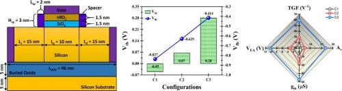
本研究展示了传统SOI n-FinFET器件的改进,结合了高k间隔和栅极堆栈(GS)工程,栅极长度为10 nm。对三种FinFET结构进行了比较,仿真结果表明,该结构在模拟性能和射频性能方面都有显著改善。模拟参数如ION/IOFF比增加了近104倍,亚阈值摆幅减少了约60%;跨导提高了~ 92%,QF提高了~ 382%,TGF提高了~ 302%,固有增益提高了近8倍,早期电压提高了近5倍,表明该器件适用于高性能CMOS电路。此外,使用截止频率、GFP、TFP等参数进行射频分析,表明所提出的配置有相当大的改进。因此,栅极堆叠和间隔层工程显著提高了FinFET的性能,增强了半导体器件的模拟和射频能力,以实现更高效的集成电路。
本文章由计算机程序翻译,如有差异,请以英文原文为准。

Performance enhancement of a spacer-engineered GS SOI n-FinFET with 10 nm gate length

Performance enhancement of a spacer-engineered GS SOI n-FinFET with 10 nm gate length
This study showcases the improvement in conventional SOI n-FinFET devices with the incorporation of a high-K spacer and gate stack (GS) engineering at 10 nm gate length. Three FinFET configurations were considered for comparison, and the simulated results show significant improvements in the analog and RF performance of the proposed configuration. Analog parameters such as the ION/IOFF ratio increased almost 104 times, subthreshold swing reduced by ∼60 %; transconductance increased by ∼92 %, QF improved by ∼382 %, TGF enhanced by ∼302 %, intrinsic gain increased by almost 8 times, and early voltage by almost 5 times, indicating the proposed device is suitable for high-performance CMOS circuits. Further, the RF analysis is performed with parameters like cut-off frequency, GFP, TFP, etc., exhibiting considerable improvement for the proposed configuration. Thus, gate stacking and spacer engineering significantly improve the FinFET performance, enhancing the analog and RF capabilities of semiconductor devices for more efficient integrated circuits.
求助全文
通过发布文献求助,成功后即可免费获取论文全文。 去求助
来源期刊
Microelectronic Engineering
Microelectronic Engineering 工程技术-工程:电子与电气
CiteScore
5.30
自引率
4.30%
发文量
131
审稿时长
29 days
期刊介绍: Microelectronic Engineering is the premier nanoprocessing, and nanotechnology journal focusing on fabrication of electronic, photonic, bioelectronic, electromechanic and fluidic devices and systems, and their applications in the broad areas of electronics, photonics, energy, life sciences, and environment. It covers also the expanding interdisciplinary field of "more than Moore" and "beyond Moore" integrated nanoelectronics / photonics and micro-/nano-/bio-systems. Through its unique mixture of peer-reviewed articles, reviews, accelerated publications, short and Technical notes, and the latest research news on key developments, Microelectronic Engineering provides comprehensive coverage of this exciting, interdisciplinary and dynamic new field for researchers in academia and professionals in industry.
×
引用
GB/T 7714-2015
复制
MLA
复制
APA
复制
导出至
BibTeX EndNote RefMan NoteFirst NoteExpress
×
提示
您的信息不完整,为了账户安全,请先补充。
现在去补充
×
提示
您因"违规操作"
具体请查看互助需知
我知道了
×
提示
确定
请完成安全验证×
copy
已复制链接
快去分享给好友吧!
我知道了
右上角分享
点击右上角分享
0
联系我们:info@booksci.cn Book学术提供免费学术资源搜索服务,方便国内外学者检索中英文文献。致力于提供最便捷和优质的服务体验。 Copyright © 2023 布克学术 All rights reserved.
京ICP备2023020795号-1
ghs 京公网安备 11010802042870号
Book学术文献互助
Book学术文献互助群
群 号:604180095
Book学术官方微信