基于BiFeO3的PLD生长层状MFIS异质结构器件的电学性能研究

IF 2.4 3区 化学 Q4 CHEMISTRY, PHYSICAL
Akshay Panchasara , Urjitsinh Rathod , Sumana Hajra , Pruthaba Jadeja , Akshay Ranpariya , Savan Katba , Vanaraj Solanki , Mahesh Jivani , Ashish Ravalia
{"title":"基于BiFeO3的PLD生长层状MFIS异质结构器件的电学性能研究","authors":"Akshay Panchasara ,&nbsp;Urjitsinh Rathod ,&nbsp;Sumana Hajra ,&nbsp;Pruthaba Jadeja ,&nbsp;Akshay Ranpariya ,&nbsp;Savan Katba ,&nbsp;Vanaraj Solanki ,&nbsp;Mahesh Jivani ,&nbsp;Ashish Ravalia","doi":"10.1016/j.chemphys.2025.112851","DOIUrl":null,"url":null,"abstract":"<div><div>The pulsed lase deposited layered based thin film heterostructured device have been fabricated in Ag (metal) / Ca doped BiFeO<sub>3</sub> (Ferroelectric) / SrTiO<sub>3</sub> (Insulator) / ZnO (Semiconductor) MFIS geometry on STO (100) single crystalline substrate. The X-ray diffraction measurement confirm the substrate-oriented growth of Ca doped BiFeO<sub>3</sub> and SrTiO<sub>3</sub> layer while growth of ZnO is in different geometry due to its different structure than substrate. Surface and microstructural characterization have been carried out using Atomic Force Microscopy measurements which indicates the homogenous grain growth of Ca doped BiFeO<sub>3</sub> and ZnO layer. Electrical properties of proposed Ca doped BiFeO<sub>3</sub> based MFIS heterostructure have been studied using frequency dependent dielectric, cyclic I-V behaviour (with and without UV illumination) and channel resistance measurements. To understand the electrical property of proposed device, various charge conduction mechanism has understood using the fitting of I-V data. In addition, role of Ca doped BiFeO<sub>3</sub> ferroelectric layer in the channel resistance is investigated.</div></div>","PeriodicalId":272,"journal":{"name":"Chemical Physics","volume":"598 ","pages":"Article 112851"},"PeriodicalIF":2.4000,"publicationDate":"2025-07-07","publicationTypes":"Journal Article","fieldsOfStudy":null,"isOpenAccess":false,"openAccessPdf":"","citationCount":"0","resultStr":"{\"title\":\"Studies on electrical properties of PLD grown BiFeO3 - based layered MFIS heterostructure device\",\"authors\":\"Akshay Panchasara ,&nbsp;Urjitsinh Rathod ,&nbsp;Sumana Hajra ,&nbsp;Pruthaba Jadeja ,&nbsp;Akshay Ranpariya ,&nbsp;Savan Katba ,&nbsp;Vanaraj Solanki ,&nbsp;Mahesh Jivani ,&nbsp;Ashish Ravalia\",\"doi\":\"10.1016/j.chemphys.2025.112851\",\"DOIUrl\":null,\"url\":null,\"abstract\":\"<div><div>The pulsed lase deposited layered based thin film heterostructured device have been fabricated in Ag (metal) / Ca doped BiFeO<sub>3</sub> (Ferroelectric) / SrTiO<sub>3</sub> (Insulator) / ZnO (Semiconductor) MFIS geometry on STO (100) single crystalline substrate. The X-ray diffraction measurement confirm the substrate-oriented growth of Ca doped BiFeO<sub>3</sub> and SrTiO<sub>3</sub> layer while growth of ZnO is in different geometry due to its different structure than substrate. Surface and microstructural characterization have been carried out using Atomic Force Microscopy measurements which indicates the homogenous grain growth of Ca doped BiFeO<sub>3</sub> and ZnO layer. Electrical properties of proposed Ca doped BiFeO<sub>3</sub> based MFIS heterostructure have been studied using frequency dependent dielectric, cyclic I-V behaviour (with and without UV illumination) and channel resistance measurements. To understand the electrical property of proposed device, various charge conduction mechanism has understood using the fitting of I-V data. In addition, role of Ca doped BiFeO<sub>3</sub> ferroelectric layer in the channel resistance is investigated.</div></div>\",\"PeriodicalId\":272,\"journal\":{\"name\":\"Chemical Physics\",\"volume\":\"598 \",\"pages\":\"Article 112851\"},\"PeriodicalIF\":2.4000,\"publicationDate\":\"2025-07-07\",\"publicationTypes\":\"Journal Article\",\"fieldsOfStudy\":null,\"isOpenAccess\":false,\"openAccessPdf\":\"\",\"citationCount\":\"0\",\"resultStr\":null,\"platform\":\"Semanticscholar\",\"paperid\":null,\"PeriodicalName\":\"Chemical Physics\",\"FirstCategoryId\":\"92\",\"ListUrlMain\":\"https://www.sciencedirect.com/science/article/pii/S0301010425002526\",\"RegionNum\":3,\"RegionCategory\":\"化学\",\"ArticlePicture\":[],\"TitleCN\":null,\"AbstractTextCN\":null,\"PMCID\":null,\"EPubDate\":\"\",\"PubModel\":\"\",\"JCR\":\"Q4\",\"JCRName\":\"CHEMISTRY, PHYSICAL\",\"Score\":null,\"Total\":0}","platform":"Semanticscholar","paperid":null,"PeriodicalName":"Chemical Physics","FirstCategoryId":"92","ListUrlMain":"https://www.sciencedirect.com/science/article/pii/S0301010425002526","RegionNum":3,"RegionCategory":"化学","ArticlePicture":[],"TitleCN":null,"AbstractTextCN":null,"PMCID":null,"EPubDate":"","PubModel":"","JCR":"Q4","JCRName":"CHEMISTRY, PHYSICAL","Score":null,"Total":0}
引用次数: 0

摘要

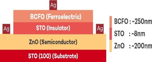
在STO(100)单晶衬底上以Ag (metal) / Ca掺杂BiFeO3 (Ferroelectric) / SrTiO3 (Insulator) / ZnO (Semiconductor) MFIS几何形状制备了脉冲激光沉积层状薄膜异质结构器件。x射线衍射测量证实了Ca掺杂BiFeO3和SrTiO3层的取向生长,而ZnO由于其与衬底的结构不同,其生长呈不同的几何形状。利用原子力显微镜对其表面和微观结构进行了表征,结果表明Ca掺杂的BiFeO3和ZnO层晶粒生长均匀。利用频率相关的介电、循环I-V行为(有和没有紫外线照射)和通道电阻测量,研究了基于Ca掺杂BiFeO3的MFIS异质结构的电学特性。为了了解所提出器件的电学性质,利用I-V数据的拟合了解了各种电荷传导机制。此外,还研究了掺钙BiFeO3铁电层对沟道电阻的影响。
本文章由计算机程序翻译,如有差异,请以英文原文为准。

Studies on electrical properties of PLD grown BiFeO3 - based layered MFIS heterostructure device

Studies on electrical properties of PLD grown BiFeO3 - based layered MFIS heterostructure device
The pulsed lase deposited layered based thin film heterostructured device have been fabricated in Ag (metal) / Ca doped BiFeO3 (Ferroelectric) / SrTiO3 (Insulator) / ZnO (Semiconductor) MFIS geometry on STO (100) single crystalline substrate. The X-ray diffraction measurement confirm the substrate-oriented growth of Ca doped BiFeO3 and SrTiO3 layer while growth of ZnO is in different geometry due to its different structure than substrate. Surface and microstructural characterization have been carried out using Atomic Force Microscopy measurements which indicates the homogenous grain growth of Ca doped BiFeO3 and ZnO layer. Electrical properties of proposed Ca doped BiFeO3 based MFIS heterostructure have been studied using frequency dependent dielectric, cyclic I-V behaviour (with and without UV illumination) and channel resistance measurements. To understand the electrical property of proposed device, various charge conduction mechanism has understood using the fitting of I-V data. In addition, role of Ca doped BiFeO3 ferroelectric layer in the channel resistance is investigated.
求助全文
通过发布文献求助,成功后即可免费获取论文全文。 去求助
来源期刊
Chemical Physics
Chemical Physics 化学-物理:原子、分子和化学物理
CiteScore
4.60
自引率
4.30%
发文量
278
审稿时长
39 days
期刊介绍: Chemical Physics publishes experimental and theoretical papers on all aspects of chemical physics. In this journal, experiments are related to theory, and in turn theoretical papers are related to present or future experiments. Subjects covered include: spectroscopy and molecular structure, interacting systems, relaxation phenomena, biological systems, materials, fundamental problems in molecular reactivity, molecular quantum theory and statistical mechanics. Computational chemistry studies of routine character are not appropriate for this journal.
×
引用
GB/T 7714-2015
复制
MLA
复制
APA
复制
导出至
BibTeX EndNote RefMan NoteFirst NoteExpress
×
提示
您的信息不完整,为了账户安全,请先补充。
现在去补充
×
提示
您因"违规操作"
具体请查看互助需知
我知道了
×
提示
确定
请完成安全验证×
copy
已复制链接
快去分享给好友吧!
我知道了
右上角分享
点击右上角分享
0
联系我们:info@booksci.cn Book学术提供免费学术资源搜索服务,方便国内外学者检索中英文文献。致力于提供最便捷和优质的服务体验。 Copyright © 2023 布克学术 All rights reserved.
京ICP备2023020795号-1
ghs 京公网安备 11010802042870号
Book学术文献互助
Book学术文献互助群
群 号:604180095
Book学术官方微信