选择性自对准溶胶-凝胶氧化铜用于大面积多值逻辑器件(Small 26/2025)

IF 12.1 2区 材料科学 Q1 CHEMISTRY, MULTIDISCIPLINARY
Small Pub Date : 2025-07-04 DOI:10.1002/smll.202570201
Seokhyeon Baek, Wonsik Kim, Won-June Lee, Jun-Gyu Choi, Sungjun Park
{"title":"选择性自对准溶胶-凝胶氧化铜用于大面积多值逻辑器件(Small 26/2025)","authors":"Seokhyeon Baek,&nbsp;Wonsik Kim,&nbsp;Won-June Lee,&nbsp;Jun-Gyu Choi,&nbsp;Sungjun Park","doi":"10.1002/smll.202570201","DOIUrl":null,"url":null,"abstract":"<p><b>Heterojunction Transistors</b></p><p>In article number 2407497, Jun-Gyu Choi, Sungjun Park, and co-workers illustrate a wafer-scale array of solution-processed heterojunction transistors fabricated via SAM-assisted selective patterning. This novel strategy highlights a promising alternative to conventional photolithography by effectively addressing the challenges posed by partially overlapped junction structures. A magnified junction interface showcases efficient carrier transport, enabled by the partially overlapped architecture of the metal oxide heterojunction.\n\n <figure>\n <div><picture>\n <source></source></picture><p></p>\n </div>\n </figure></p>","PeriodicalId":228,"journal":{"name":"Small","volume":"21 26","pages":""},"PeriodicalIF":12.1000,"publicationDate":"2025-07-04","publicationTypes":"Journal Article","fieldsOfStudy":null,"isOpenAccess":false,"openAccessPdf":"https://onlinelibrary.wiley.com/doi/epdf/10.1002/smll.202570201","citationCount":"0","resultStr":"{\"title\":\"Selectively Self-Aligned Sol-Gel Copper Oxide for Large-Area Multi-Valued Logic Devices (Small 26/2025)\",\"authors\":\"Seokhyeon Baek,&nbsp;Wonsik Kim,&nbsp;Won-June Lee,&nbsp;Jun-Gyu Choi,&nbsp;Sungjun Park\",\"doi\":\"10.1002/smll.202570201\",\"DOIUrl\":null,\"url\":null,\"abstract\":\"<p><b>Heterojunction Transistors</b></p><p>In article number 2407497, Jun-Gyu Choi, Sungjun Park, and co-workers illustrate a wafer-scale array of solution-processed heterojunction transistors fabricated via SAM-assisted selective patterning. This novel strategy highlights a promising alternative to conventional photolithography by effectively addressing the challenges posed by partially overlapped junction structures. A magnified junction interface showcases efficient carrier transport, enabled by the partially overlapped architecture of the metal oxide heterojunction.\\n\\n <figure>\\n <div><picture>\\n <source></source></picture><p></p>\\n </div>\\n </figure></p>\",\"PeriodicalId\":228,\"journal\":{\"name\":\"Small\",\"volume\":\"21 26\",\"pages\":\"\"},\"PeriodicalIF\":12.1000,\"publicationDate\":\"2025-07-04\",\"publicationTypes\":\"Journal Article\",\"fieldsOfStudy\":null,\"isOpenAccess\":false,\"openAccessPdf\":\"https://onlinelibrary.wiley.com/doi/epdf/10.1002/smll.202570201\",\"citationCount\":\"0\",\"resultStr\":null,\"platform\":\"Semanticscholar\",\"paperid\":null,\"PeriodicalName\":\"Small\",\"FirstCategoryId\":\"88\",\"ListUrlMain\":\"https://onlinelibrary.wiley.com/doi/10.1002/smll.202570201\",\"RegionNum\":2,\"RegionCategory\":\"材料科学\",\"ArticlePicture\":[],\"TitleCN\":null,\"AbstractTextCN\":null,\"PMCID\":null,\"EPubDate\":\"\",\"PubModel\":\"\",\"JCR\":\"Q1\",\"JCRName\":\"CHEMISTRY, MULTIDISCIPLINARY\",\"Score\":null,\"Total\":0}","platform":"Semanticscholar","paperid":null,"PeriodicalName":"Small","FirstCategoryId":"88","ListUrlMain":"https://onlinelibrary.wiley.com/doi/10.1002/smll.202570201","RegionNum":2,"RegionCategory":"材料科学","ArticlePicture":[],"TitleCN":null,"AbstractTextCN":null,"PMCID":null,"EPubDate":"","PubModel":"","JCR":"Q1","JCRName":"CHEMISTRY, MULTIDISCIPLINARY","Score":null,"Total":0}
引用次数: 0

摘要

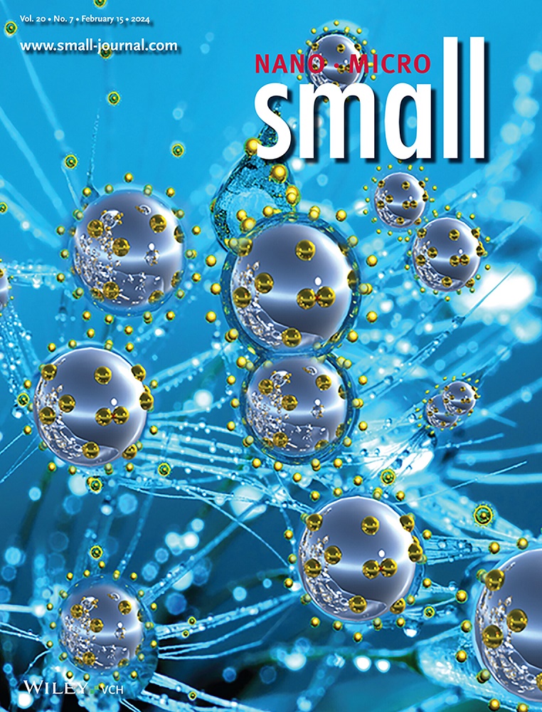
异质结晶体管在文章编号2407497中,Jun-Gyu Choi, Sungjun Park及其同事展示了通过sam辅助选择性图像化制造的晶圆级溶液处理异质结晶体管阵列。这种新颖的策略通过有效地解决部分重叠结结构带来的挑战,突出了传统光刻技术的一个有希望的替代方案。放大的结界面展示了高效的载流子传输,这是由金属氧化物异质结的部分重叠结构实现的。
本文章由计算机程序翻译,如有差异,请以英文原文为准。

Selectively Self-Aligned Sol-Gel Copper Oxide for Large-Area Multi-Valued Logic Devices (Small 26/2025)

Selectively Self-Aligned Sol-Gel Copper Oxide for Large-Area Multi-Valued Logic Devices (Small 26/2025)

Heterojunction Transistors

In article number 2407497, Jun-Gyu Choi, Sungjun Park, and co-workers illustrate a wafer-scale array of solution-processed heterojunction transistors fabricated via SAM-assisted selective patterning. This novel strategy highlights a promising alternative to conventional photolithography by effectively addressing the challenges posed by partially overlapped junction structures. A magnified junction interface showcases efficient carrier transport, enabled by the partially overlapped architecture of the metal oxide heterojunction.

求助全文
通过发布文献求助,成功后即可免费获取论文全文。 去求助
来源期刊
Small
Small 工程技术-材料科学:综合
CiteScore
17.70
自引率
3.80%
发文量
1830
审稿时长
2.1 months
期刊介绍: Small serves as an exceptional platform for both experimental and theoretical studies in fundamental and applied interdisciplinary research at the nano- and microscale. The journal offers a compelling mix of peer-reviewed Research Articles, Reviews, Perspectives, and Comments. With a remarkable 2022 Journal Impact Factor of 13.3 (Journal Citation Reports from Clarivate Analytics, 2023), Small remains among the top multidisciplinary journals, covering a wide range of topics at the interface of materials science, chemistry, physics, engineering, medicine, and biology. Small's readership includes biochemists, biologists, biomedical scientists, chemists, engineers, information technologists, materials scientists, physicists, and theoreticians alike.
×
引用
GB/T 7714-2015
复制
MLA
复制
APA
复制
导出至
BibTeX EndNote RefMan NoteFirst NoteExpress
×
提示
您的信息不完整,为了账户安全,请先补充。
现在去补充
×
提示
您因"违规操作"
具体请查看互助需知
我知道了
×
提示
确定
请完成安全验证×
copy
已复制链接
快去分享给好友吧!
我知道了
右上角分享
点击右上角分享
0
联系我们:info@booksci.cn Book学术提供免费学术资源搜索服务,方便国内外学者检索中英文文献。致力于提供最便捷和优质的服务体验。 Copyright © 2023 布克学术 All rights reserved.
京ICP备2023020795号-1
ghs 京公网安备 11010802042870号
Book学术文献互助
Book学术文献互助群
群 号:604180095
Book学术官方微信