Jeff J. P. M. Schulpen, Saravana B. Basuvalingam, Marcel A. Verheijen and Ageeth A. Bol
{"title":"二维WS2在三维纳米结构上的适形限制","authors":"Jeff J. P. M. Schulpen, Saravana B. Basuvalingam, Marcel A. Verheijen and Ageeth A. Bol","doi":"10.1039/D5NR01013F","DOIUrl":null,"url":null,"abstract":"<p >3D nanostructures are a vital part of various applications envisaged for two-dimensional transition metal dichalcogenides (2D TMDs), such as nanoelectronics and catalysis. However, achieving conformal deposition of 2D TMD films on 3D nanostructures is challenging due to the requirement for bending the basal planes of the 2D TMDs. Here, the limits of conformality of 2D WS<small><sub>2</sub></small> deposited by atomic layer deposition on SiO<small><sub>2</sub></small> 3D nanostructures are investigated through cross-sectional transmission electron microscopy imaging. A minimum radius of curvature of 4 nm is identified above which basal plane conformality is almost always observed, while for smaller radii conformality is only observed in approximately half of the cases. We show that the observed tipping point agrees with the balance between the adhesion and stiffness forces, which allows for the estimation of the critical radius of curvature for other 2D TMDs and substrates. These results provide guidelines for the design of 3D nanostructured devices and substrates on which conformality of 2D materials is desired.</p>","PeriodicalId":92,"journal":{"name":"Nanoscale","volume":" 28","pages":" 16922-16927"},"PeriodicalIF":5.1000,"publicationDate":"2025-07-01","publicationTypes":"Journal Article","fieldsOfStudy":null,"isOpenAccess":false,"openAccessPdf":"https://pubs.rsc.org/en/content/articlepdf/2025/nr/d5nr01013f?page=search","citationCount":"0","resultStr":"{\"title\":\"Conformality limits of 2D WS2 on 3D nanostructures†\",\"authors\":\"Jeff J. P. M. Schulpen, Saravana B. Basuvalingam, Marcel A. Verheijen and Ageeth A. Bol\",\"doi\":\"10.1039/D5NR01013F\",\"DOIUrl\":null,\"url\":null,\"abstract\":\"<p >3D nanostructures are a vital part of various applications envisaged for two-dimensional transition metal dichalcogenides (2D TMDs), such as nanoelectronics and catalysis. However, achieving conformal deposition of 2D TMD films on 3D nanostructures is challenging due to the requirement for bending the basal planes of the 2D TMDs. Here, the limits of conformality of 2D WS<small><sub>2</sub></small> deposited by atomic layer deposition on SiO<small><sub>2</sub></small> 3D nanostructures are investigated through cross-sectional transmission electron microscopy imaging. A minimum radius of curvature of 4 nm is identified above which basal plane conformality is almost always observed, while for smaller radii conformality is only observed in approximately half of the cases. We show that the observed tipping point agrees with the balance between the adhesion and stiffness forces, which allows for the estimation of the critical radius of curvature for other 2D TMDs and substrates. These results provide guidelines for the design of 3D nanostructured devices and substrates on which conformality of 2D materials is desired.</p>\",\"PeriodicalId\":92,\"journal\":{\"name\":\"Nanoscale\",\"volume\":\" 28\",\"pages\":\" 16922-16927\"},\"PeriodicalIF\":5.1000,\"publicationDate\":\"2025-07-01\",\"publicationTypes\":\"Journal Article\",\"fieldsOfStudy\":null,\"isOpenAccess\":false,\"openAccessPdf\":\"https://pubs.rsc.org/en/content/articlepdf/2025/nr/d5nr01013f?page=search\",\"citationCount\":\"0\",\"resultStr\":null,\"platform\":\"Semanticscholar\",\"paperid\":null,\"PeriodicalName\":\"Nanoscale\",\"FirstCategoryId\":\"88\",\"ListUrlMain\":\"https://pubs.rsc.org/en/content/articlelanding/2025/nr/d5nr01013f\",\"RegionNum\":3,\"RegionCategory\":\"材料科学\",\"ArticlePicture\":[],\"TitleCN\":null,\"AbstractTextCN\":null,\"PMCID\":null,\"EPubDate\":\"\",\"PubModel\":\"\",\"JCR\":\"Q1\",\"JCRName\":\"CHEMISTRY, MULTIDISCIPLINARY\",\"Score\":null,\"Total\":0}","platform":"Semanticscholar","paperid":null,"PeriodicalName":"Nanoscale","FirstCategoryId":"88","ListUrlMain":"https://pubs.rsc.org/en/content/articlelanding/2025/nr/d5nr01013f","RegionNum":3,"RegionCategory":"材料科学","ArticlePicture":[],"TitleCN":null,"AbstractTextCN":null,"PMCID":null,"EPubDate":"","PubModel":"","JCR":"Q1","JCRName":"CHEMISTRY, MULTIDISCIPLINARY","Score":null,"Total":0}
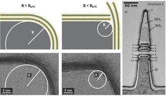
Conformality limits of 2D WS2 on 3D nanostructures†
3D nanostructures are a vital part of various applications envisaged for two-dimensional transition metal dichalcogenides (2D TMDs), such as nanoelectronics and catalysis. However, achieving conformal deposition of 2D TMD films on 3D nanostructures is challenging due to the requirement for bending the basal planes of the 2D TMDs. Here, the limits of conformality of 2D WS2 deposited by atomic layer deposition on SiO2 3D nanostructures are investigated through cross-sectional transmission electron microscopy imaging. A minimum radius of curvature of 4 nm is identified above which basal plane conformality is almost always observed, while for smaller radii conformality is only observed in approximately half of the cases. We show that the observed tipping point agrees with the balance between the adhesion and stiffness forces, which allows for the estimation of the critical radius of curvature for other 2D TMDs and substrates. These results provide guidelines for the design of 3D nanostructured devices and substrates on which conformality of 2D materials is desired.
期刊介绍:
Nanoscale is a high-impact international journal, publishing high-quality research across nanoscience and nanotechnology. Nanoscale publishes a full mix of research articles on experimental and theoretical work, including reviews, communications, and full papers.Highly interdisciplinary, this journal appeals to scientists, researchers and professionals interested in nanoscience and nanotechnology, quantum materials and quantum technology, including the areas of physics, chemistry, biology, medicine, materials, energy/environment, information technology, detection science, healthcare and drug discovery, and electronics.

 求助内容:
求助内容: 应助结果提醒方式:


