Xiaotian Sun*, Shibo Fang, Ge Zhang, Linqiang Xu, Yee Sin Ang, Shujing Zhu, Qiang Li, Xingyue Yang, Zongmeng Yang, Junfeng Li, Weizhou Wang*, Zhigang Song* and Jing Lu*,
{"title":"面向未来技术节点的单层WS2亚5nm晶体管:理论研究","authors":"Xiaotian Sun*, Shibo Fang, Ge Zhang, Linqiang Xu, Yee Sin Ang, Shujing Zhu, Qiang Li, Xingyue Yang, Zongmeng Yang, Junfeng Li, Weizhou Wang*, Zhigang Song* and Jing Lu*, ","doi":"10.1021/acsanm.5c0141810.1021/acsanm.5c01418","DOIUrl":null,"url":null,"abstract":"<p >Motivated by realizing the excellent device performance of the 10 nm channel-length MoS<sub>2</sub> field-effect transistors [ <cite><i>Nature Electronics</i></cite> <span>2024</span>, <em>7</em>, 545–556], we explore the device performance limit of the monolayer (ML) WS<sub>2</sub> transistors in the sub-5 nm region through <i>ab initio</i> quantum transport simulations. We find that both the optimized n- and p-type ML WS<sub>2</sub> metal oxide semiconductor field-effect transistors (MOSFETs) can satisfy the key performance metrics for high-performance applications of the International Technology Roadmap (ITRS) when the gate length is reduced to 3 nm. In addition, the performance of both the n- and p-type ML WS<sub>2</sub> MOSFETs is better than that of the MoS<sub>2</sub> counterparts for high-performance applications. Notably, at a gate length of 5 nm, the key performance metrics of high-performance and low-power ML WS<sub>2</sub> devices show excellent n–p symmetry, indicating their potential for complementary metal oxide semiconductor (CMOS) applications. Our work indicates that the ML WS<sub>2</sub> is a promising candidate as a channel material for prolonging Moore’s law in the future.</p>","PeriodicalId":6,"journal":{"name":"ACS Applied Nano Materials","volume":"8 24","pages":"12594–12607 12594–12607"},"PeriodicalIF":5.5000,"publicationDate":"2025-06-05","publicationTypes":"Journal Article","fieldsOfStudy":null,"isOpenAccess":false,"openAccessPdf":"","citationCount":"0","resultStr":"{\"title\":\"Monolayer WS2 Sub-5 nm Transistor for Future Technology Nodes: A Theoretical Study\",\"authors\":\"Xiaotian Sun*, Shibo Fang, Ge Zhang, Linqiang Xu, Yee Sin Ang, Shujing Zhu, Qiang Li, Xingyue Yang, Zongmeng Yang, Junfeng Li, Weizhou Wang*, Zhigang Song* and Jing Lu*, \",\"doi\":\"10.1021/acsanm.5c0141810.1021/acsanm.5c01418\",\"DOIUrl\":null,\"url\":null,\"abstract\":\"<p >Motivated by realizing the excellent device performance of the 10 nm channel-length MoS<sub>2</sub> field-effect transistors [ <cite><i>Nature Electronics</i></cite> <span>2024</span>, <em>7</em>, 545–556], we explore the device performance limit of the monolayer (ML) WS<sub>2</sub> transistors in the sub-5 nm region through <i>ab initio</i> quantum transport simulations. We find that both the optimized n- and p-type ML WS<sub>2</sub> metal oxide semiconductor field-effect transistors (MOSFETs) can satisfy the key performance metrics for high-performance applications of the International Technology Roadmap (ITRS) when the gate length is reduced to 3 nm. In addition, the performance of both the n- and p-type ML WS<sub>2</sub> MOSFETs is better than that of the MoS<sub>2</sub> counterparts for high-performance applications. Notably, at a gate length of 5 nm, the key performance metrics of high-performance and low-power ML WS<sub>2</sub> devices show excellent n–p symmetry, indicating their potential for complementary metal oxide semiconductor (CMOS) applications. Our work indicates that the ML WS<sub>2</sub> is a promising candidate as a channel material for prolonging Moore’s law in the future.</p>\",\"PeriodicalId\":6,\"journal\":{\"name\":\"ACS Applied Nano Materials\",\"volume\":\"8 24\",\"pages\":\"12594–12607 12594–12607\"},\"PeriodicalIF\":5.5000,\"publicationDate\":\"2025-06-05\",\"publicationTypes\":\"Journal Article\",\"fieldsOfStudy\":null,\"isOpenAccess\":false,\"openAccessPdf\":\"\",\"citationCount\":\"0\",\"resultStr\":null,\"platform\":\"Semanticscholar\",\"paperid\":null,\"PeriodicalName\":\"ACS Applied Nano Materials\",\"FirstCategoryId\":\"88\",\"ListUrlMain\":\"https://pubs.acs.org/doi/10.1021/acsanm.5c01418\",\"RegionNum\":2,\"RegionCategory\":\"材料科学\",\"ArticlePicture\":[],\"TitleCN\":null,\"AbstractTextCN\":null,\"PMCID\":null,\"EPubDate\":\"\",\"PubModel\":\"\",\"JCR\":\"Q2\",\"JCRName\":\"MATERIALS SCIENCE, MULTIDISCIPLINARY\",\"Score\":null,\"Total\":0}","platform":"Semanticscholar","paperid":null,"PeriodicalName":"ACS Applied Nano Materials","FirstCategoryId":"88","ListUrlMain":"https://pubs.acs.org/doi/10.1021/acsanm.5c01418","RegionNum":2,"RegionCategory":"材料科学","ArticlePicture":[],"TitleCN":null,"AbstractTextCN":null,"PMCID":null,"EPubDate":"","PubModel":"","JCR":"Q2","JCRName":"MATERIALS SCIENCE, MULTIDISCIPLINARY","Score":null,"Total":0}
Monolayer WS2 Sub-5 nm Transistor for Future Technology Nodes: A Theoretical Study
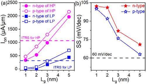
Motivated by realizing the excellent device performance of the 10 nm channel-length MoS2 field-effect transistors [ Nature Electronics2024, 7, 545–556], we explore the device performance limit of the monolayer (ML) WS2 transistors in the sub-5 nm region through ab initio quantum transport simulations. We find that both the optimized n- and p-type ML WS2 metal oxide semiconductor field-effect transistors (MOSFETs) can satisfy the key performance metrics for high-performance applications of the International Technology Roadmap (ITRS) when the gate length is reduced to 3 nm. In addition, the performance of both the n- and p-type ML WS2 MOSFETs is better than that of the MoS2 counterparts for high-performance applications. Notably, at a gate length of 5 nm, the key performance metrics of high-performance and low-power ML WS2 devices show excellent n–p symmetry, indicating their potential for complementary metal oxide semiconductor (CMOS) applications. Our work indicates that the ML WS2 is a promising candidate as a channel material for prolonging Moore’s law in the future.
期刊介绍:
ACS Applied Nano Materials is an interdisciplinary journal publishing original research covering all aspects of engineering, chemistry, physics and biology relevant to applications of nanomaterials. The journal is devoted to reports of new and original experimental and theoretical research of an applied nature that integrate knowledge in the areas of materials, engineering, physics, bioscience, and chemistry into important applications of nanomaterials.

 求助内容:
求助内容: 应助结果提醒方式:


