Bhishma Pandit, Jungwoo Bong, Seongwon Lee, Jungwoo Lee, Sameer Pokhrel, Hagyoul Bae, Ji-Wan Kim, Yunjo Jeong, Sangmin An, Jaehee Cho, Chel-Jong Choi, Krishna Moorthy Ponnusamy, S. Chandramohan, Hyeon-Sik Jang* and Keun Heo*,
{"title":"晶圆级单层二硫化钼高探测率宽带金属-半导体-金属光电探测器阵列的光探测机理和紫外-可见光成像特性","authors":"Bhishma Pandit, Jungwoo Bong, Seongwon Lee, Jungwoo Lee, Sameer Pokhrel, Hagyoul Bae, Ji-Wan Kim, Yunjo Jeong, Sangmin An, Jaehee Cho, Chel-Jong Choi, Krishna Moorthy Ponnusamy, S. Chandramohan, Hyeon-Sik Jang* and Keun Heo*, ","doi":"10.1021/acsami.5c0460210.1021/acsami.5c04602","DOIUrl":null,"url":null,"abstract":"<p >The discovery of an intrinsic direct bandgap in single-layer MoS<sub>2</sub> has revealed significant potential for advancements in optoelectronic and photonic applications. This study aims to explore this potential by developing a high-performance Ni/Au metal–semiconductor–metal photodetector on wafer-scale epitaxially grown MoS<sub>2</sub>. The quality of the monolayer MoS<sub>2</sub> film was verified using various techniques, including Raman, photoluminescence (PL), atomic force microscopy (AFM), X-ray photoelectron spectroscopy (XPS), and transmission electron microscopy (TEM). Results showed a high photoresponse of 2.06 and 0.68 A/W under 350 and 650 nm light illumination, respectively, at a 10 V reverse bias, along with an ultralow dark current measured in picoamps. These results indicate a low noise level and high photo-to-dark current rejection ratios of 5.45 × 10<sup>4</sup> and 3.41 × 10<sup>4</sup> under 350 and 650 nm illumination, respectively. The photodetector exhibited a maximum detectivity of 5.1 × 10<sup>16</sup> cm Hz<sup>1/2</sup> W<sup>–1</sup> at 5 V under 350 nm of UV illumination, and the quantum efficiency surpassed 100% when the reverse bias voltage exceeded 3 V, demonstrating gain manifestation within the device. The dominance of a trap-assisted photoconductive gain mechanism was suggested by the power law exponent and the temporal characteristics observed. UV and visible imaging capabilities were also demonstrated using a “MoS2”-printed shadow mask and a single metal–semiconductor–metal (MSM) photodetector. This study highlights the superior photoimaging capabilities of the MoS<sub>2</sub> MSM photodetector, offering substantial contributions to the field of optoelectronics and suggesting practical applications in photonic devices.</p>","PeriodicalId":5,"journal":{"name":"ACS Applied Materials & Interfaces","volume":"17 24","pages":"35732–35742 35732–35742"},"PeriodicalIF":8.2000,"publicationDate":"2025-06-06","publicationTypes":"Journal Article","fieldsOfStudy":null,"isOpenAccess":false,"openAccessPdf":"","citationCount":"0","resultStr":"{\"title\":\"Photodetection Mechanisms and Ultraviolet–Visible Imaging Characteristics of High-Detectivity Broadband Metal–Semiconductor–Metal Photodetector Arrays on Wafer-Scale Monolayer MoS2\",\"authors\":\"Bhishma Pandit, Jungwoo Bong, Seongwon Lee, Jungwoo Lee, Sameer Pokhrel, Hagyoul Bae, Ji-Wan Kim, Yunjo Jeong, Sangmin An, Jaehee Cho, Chel-Jong Choi, Krishna Moorthy Ponnusamy, S. Chandramohan, Hyeon-Sik Jang* and Keun Heo*, \",\"doi\":\"10.1021/acsami.5c0460210.1021/acsami.5c04602\",\"DOIUrl\":null,\"url\":null,\"abstract\":\"<p >The discovery of an intrinsic direct bandgap in single-layer MoS<sub>2</sub> has revealed significant potential for advancements in optoelectronic and photonic applications. This study aims to explore this potential by developing a high-performance Ni/Au metal–semiconductor–metal photodetector on wafer-scale epitaxially grown MoS<sub>2</sub>. The quality of the monolayer MoS<sub>2</sub> film was verified using various techniques, including Raman, photoluminescence (PL), atomic force microscopy (AFM), X-ray photoelectron spectroscopy (XPS), and transmission electron microscopy (TEM). Results showed a high photoresponse of 2.06 and 0.68 A/W under 350 and 650 nm light illumination, respectively, at a 10 V reverse bias, along with an ultralow dark current measured in picoamps. These results indicate a low noise level and high photo-to-dark current rejection ratios of 5.45 × 10<sup>4</sup> and 3.41 × 10<sup>4</sup> under 350 and 650 nm illumination, respectively. The photodetector exhibited a maximum detectivity of 5.1 × 10<sup>16</sup> cm Hz<sup>1/2</sup> W<sup>–1</sup> at 5 V under 350 nm of UV illumination, and the quantum efficiency surpassed 100% when the reverse bias voltage exceeded 3 V, demonstrating gain manifestation within the device. The dominance of a trap-assisted photoconductive gain mechanism was suggested by the power law exponent and the temporal characteristics observed. UV and visible imaging capabilities were also demonstrated using a “MoS2”-printed shadow mask and a single metal–semiconductor–metal (MSM) photodetector. This study highlights the superior photoimaging capabilities of the MoS<sub>2</sub> MSM photodetector, offering substantial contributions to the field of optoelectronics and suggesting practical applications in photonic devices.</p>\",\"PeriodicalId\":5,\"journal\":{\"name\":\"ACS Applied Materials & Interfaces\",\"volume\":\"17 24\",\"pages\":\"35732–35742 35732–35742\"},\"PeriodicalIF\":8.2000,\"publicationDate\":\"2025-06-06\",\"publicationTypes\":\"Journal Article\",\"fieldsOfStudy\":null,\"isOpenAccess\":false,\"openAccessPdf\":\"\",\"citationCount\":\"0\",\"resultStr\":null,\"platform\":\"Semanticscholar\",\"paperid\":null,\"PeriodicalName\":\"ACS Applied Materials & Interfaces\",\"FirstCategoryId\":\"88\",\"ListUrlMain\":\"https://pubs.acs.org/doi/10.1021/acsami.5c04602\",\"RegionNum\":2,\"RegionCategory\":\"材料科学\",\"ArticlePicture\":[],\"TitleCN\":null,\"AbstractTextCN\":null,\"PMCID\":null,\"EPubDate\":\"\",\"PubModel\":\"\",\"JCR\":\"Q1\",\"JCRName\":\"MATERIALS SCIENCE, MULTIDISCIPLINARY\",\"Score\":null,\"Total\":0}","platform":"Semanticscholar","paperid":null,"PeriodicalName":"ACS Applied Materials & Interfaces","FirstCategoryId":"88","ListUrlMain":"https://pubs.acs.org/doi/10.1021/acsami.5c04602","RegionNum":2,"RegionCategory":"材料科学","ArticlePicture":[],"TitleCN":null,"AbstractTextCN":null,"PMCID":null,"EPubDate":"","PubModel":"","JCR":"Q1","JCRName":"MATERIALS SCIENCE, MULTIDISCIPLINARY","Score":null,"Total":0}
引用次数: 0
摘要
单层二硫化钼固有直接带隙的发现揭示了光电和光子应用的重大潜力。本研究旨在通过在晶圆级外延生长的MoS2上开发高性能Ni/Au金属-半导体-金属光电探测器来探索这种潜力。利用拉曼、光致发光(PL)、原子力显微镜(AFM)、x射线光电子能谱(XPS)和透射电子显微镜(TEM)等多种技术验证了单层MoS2薄膜的质量。结果表明,在350 nm和650 nm光照下,在10 V反向偏置下,在以皮安为单位的超低暗电流下,其光响应分别为2.06和0.68 a /W。这些结果表明,在350 nm和650 nm照明下,该材料具有低噪声水平和高光暗抑制比,分别为5.45 × 10⁴和3.41 × 10⁴。在350 nm紫外光照射下,该光电探测器在5v下的最大检出率为5.1 × 1016 cm Hz1/2 W-1,当反向偏置电压超过3v时,量子效率超过100%,在器件内表现出增益表现。幂律指数和观察到的时间特征表明,陷阱辅助光导增益机制占主导地位。使用“二硫化钼”印刷的阴影掩膜和单一金属-半导体-金属(MSM)光电探测器也演示了紫外和可见光成像能力。该研究突出了MoS2 MSM光电探测器优越的光电成像能力,为光电子学领域做出了重大贡献,并提出了在光子器件中的实际应用。
Photodetection Mechanisms and Ultraviolet–Visible Imaging Characteristics of High-Detectivity Broadband Metal–Semiconductor–Metal Photodetector Arrays on Wafer-Scale Monolayer MoS2
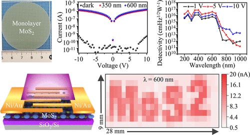
The discovery of an intrinsic direct bandgap in single-layer MoS2 has revealed significant potential for advancements in optoelectronic and photonic applications. This study aims to explore this potential by developing a high-performance Ni/Au metal–semiconductor–metal photodetector on wafer-scale epitaxially grown MoS2. The quality of the monolayer MoS2 film was verified using various techniques, including Raman, photoluminescence (PL), atomic force microscopy (AFM), X-ray photoelectron spectroscopy (XPS), and transmission electron microscopy (TEM). Results showed a high photoresponse of 2.06 and 0.68 A/W under 350 and 650 nm light illumination, respectively, at a 10 V reverse bias, along with an ultralow dark current measured in picoamps. These results indicate a low noise level and high photo-to-dark current rejection ratios of 5.45 × 10⁴ and 3.41 × 10⁴ under 350 and 650 nm illumination, respectively. The photodetector exhibited a maximum detectivity of 5.1 × 1016 cm Hz1/2 W–1 at 5 V under 350 nm of UV illumination, and the quantum efficiency surpassed 100% when the reverse bias voltage exceeded 3 V, demonstrating gain manifestation within the device. The dominance of a trap-assisted photoconductive gain mechanism was suggested by the power law exponent and the temporal characteristics observed. UV and visible imaging capabilities were also demonstrated using a “MoS2”-printed shadow mask and a single metal–semiconductor–metal (MSM) photodetector. This study highlights the superior photoimaging capabilities of the MoS2 MSM photodetector, offering substantial contributions to the field of optoelectronics and suggesting practical applications in photonic devices.
期刊介绍:
ACS Applied Materials & Interfaces is a leading interdisciplinary journal that brings together chemists, engineers, physicists, and biologists to explore the development and utilization of newly-discovered materials and interfacial processes for specific applications. Our journal has experienced remarkable growth since its establishment in 2009, both in terms of the number of articles published and the impact of the research showcased. We are proud to foster a truly global community, with the majority of published articles originating from outside the United States, reflecting the rapid growth of applied research worldwide.

 求助内容:
求助内容: 应助结果提醒方式:


