Yi Li, Yan Guo, Jin Li, Meiqi Xi, Lan Bai, Jianfeng Zhang, Shu Li, Xuehao Zhu, Yinghua He, Bingyu He, Xingxing Chen, Yuting Zhang, Yujia Gong, Zilun Yin, Jiahao Kang, Lian-Mao Peng, Rong Zhang, Yugang Zhou*, Yu Cao* and Xuelei Liang*,
{"title":"碳纳米管有源矩阵背板驱动的微型led微显示器","authors":"Yi Li, Yan Guo, Jin Li, Meiqi Xi, Lan Bai, Jianfeng Zhang, Shu Li, Xuehao Zhu, Yinghua He, Bingyu He, Xingxing Chen, Yuting Zhang, Yujia Gong, Zilun Yin, Jiahao Kang, Lian-Mao Peng, Rong Zhang, Yugang Zhou*, Yu Cao* and Xuelei Liang*, ","doi":"10.1021/acsnano.5c00672","DOIUrl":null,"url":null,"abstract":"<p >Micro-light-emitting-diodes (μLEDs) are poised to revolutionize flat-panel display (FPD) technology with their exceptional brightness, contrast ratio, energy efficiency, and ultrahigh resolutions, making them indispensable for augmented reality (AR) and virtual reality (VR) microdisplays. However, the realization of high pixel-per-inch (PPI) μLED microdisplays demands advanced thin-film transistor (TFT) backplanes with robust driving capabilities. Presently, single-crystalline silicon CMOS dominates the industry for this application, but its nontransparent nature, wafer size limitations, and high fabrication cost restrict its scalability. Alternative technologies, including low-temperature polycrystalline silicon (LTPS) and metal oxide semiconductors, fail to deliver the required small device dimensions, driving performance, and stability. Two-dimensional transition metal dichalcogenides (TMDs) have shown potential, but their integration has faced challenges, such as complex transfer processes and limited scalability, resulting in only semiactive-matrix display demonstrations. Here, we present a prototype active-matrix (AM) μLED microdisplay driven by optimized carbon nanotube (CNT) TFTs with Al<sub>2</sub>O<sub>3</sub>/SiO<sub>2</sub> gate dielectric stack and Y<sub>2</sub>O<sub>3</sub>/SiO<sub>2</sub>/polyimide passivation layers. Our CNT TFTs with a channel length (<i>L</i><sub>ch</sub>) of 3 μm achieve a driving current of ∼10 μA/μm and a mobility of ∼27 cm<sup>2</sup>/(V·s), while scaling <i>L</i><sub>ch</sub> to 0.5 μm enhances the driving current to ∼80 μA/μm and a mobility of ∼40 cm<sup>2</sup>/(V·s), surpassing most previously reported CNT TFTs for AM displays and enabling AM-μLED microdisplays with a PPI up to 3400. Moreover, a heterogeneous integration process ultilizing flip-chip eutectic bonding was developed to assemble μLED arrays onto CNT TFT backplanes, achieving a yield of ∼100% aided by the PI layer. Furthermore, CNT TFT-based two-transistor, one-capacitor (2T1C) pixel-driving circuits and peripheral control circuits were designed to support both pulse amplitude modulation (PAM) and pulse width modulation (PWM) of μLED operation. These advancements culminate in a 32 × 32-pixel AM-μLED prototype microdisplay with a PPI of 357, capable of dynamic image and video display. Our work demonstrates CNT TFTs as a viable and scalable solution for next-generation μLED microdisplays.</p>","PeriodicalId":21,"journal":{"name":"ACS Nano","volume":"19 25","pages":"22837–22848"},"PeriodicalIF":16.0000,"publicationDate":"2025-06-13","publicationTypes":"Journal Article","fieldsOfStudy":null,"isOpenAccess":false,"openAccessPdf":"","citationCount":"0","resultStr":"{\"title\":\"Micro-LED Microdisplays Driven by Carbon Nanotube Active-Matrix Backplanes\",\"authors\":\"Yi Li, Yan Guo, Jin Li, Meiqi Xi, Lan Bai, Jianfeng Zhang, Shu Li, Xuehao Zhu, Yinghua He, Bingyu He, Xingxing Chen, Yuting Zhang, Yujia Gong, Zilun Yin, Jiahao Kang, Lian-Mao Peng, Rong Zhang, Yugang Zhou*, Yu Cao* and Xuelei Liang*, \",\"doi\":\"10.1021/acsnano.5c00672\",\"DOIUrl\":null,\"url\":null,\"abstract\":\"<p >Micro-light-emitting-diodes (μLEDs) are poised to revolutionize flat-panel display (FPD) technology with their exceptional brightness, contrast ratio, energy efficiency, and ultrahigh resolutions, making them indispensable for augmented reality (AR) and virtual reality (VR) microdisplays. However, the realization of high pixel-per-inch (PPI) μLED microdisplays demands advanced thin-film transistor (TFT) backplanes with robust driving capabilities. Presently, single-crystalline silicon CMOS dominates the industry for this application, but its nontransparent nature, wafer size limitations, and high fabrication cost restrict its scalability. Alternative technologies, including low-temperature polycrystalline silicon (LTPS) and metal oxide semiconductors, fail to deliver the required small device dimensions, driving performance, and stability. Two-dimensional transition metal dichalcogenides (TMDs) have shown potential, but their integration has faced challenges, such as complex transfer processes and limited scalability, resulting in only semiactive-matrix display demonstrations. Here, we present a prototype active-matrix (AM) μLED microdisplay driven by optimized carbon nanotube (CNT) TFTs with Al<sub>2</sub>O<sub>3</sub>/SiO<sub>2</sub> gate dielectric stack and Y<sub>2</sub>O<sub>3</sub>/SiO<sub>2</sub>/polyimide passivation layers. Our CNT TFTs with a channel length (<i>L</i><sub>ch</sub>) of 3 μm achieve a driving current of ∼10 μA/μm and a mobility of ∼27 cm<sup>2</sup>/(V·s), while scaling <i>L</i><sub>ch</sub> to 0.5 μm enhances the driving current to ∼80 μA/μm and a mobility of ∼40 cm<sup>2</sup>/(V·s), surpassing most previously reported CNT TFTs for AM displays and enabling AM-μLED microdisplays with a PPI up to 3400. Moreover, a heterogeneous integration process ultilizing flip-chip eutectic bonding was developed to assemble μLED arrays onto CNT TFT backplanes, achieving a yield of ∼100% aided by the PI layer. Furthermore, CNT TFT-based two-transistor, one-capacitor (2T1C) pixel-driving circuits and peripheral control circuits were designed to support both pulse amplitude modulation (PAM) and pulse width modulation (PWM) of μLED operation. These advancements culminate in a 32 × 32-pixel AM-μLED prototype microdisplay with a PPI of 357, capable of dynamic image and video display. Our work demonstrates CNT TFTs as a viable and scalable solution for next-generation μLED microdisplays.</p>\",\"PeriodicalId\":21,\"journal\":{\"name\":\"ACS Nano\",\"volume\":\"19 25\",\"pages\":\"22837–22848\"},\"PeriodicalIF\":16.0000,\"publicationDate\":\"2025-06-13\",\"publicationTypes\":\"Journal Article\",\"fieldsOfStudy\":null,\"isOpenAccess\":false,\"openAccessPdf\":\"\",\"citationCount\":\"0\",\"resultStr\":null,\"platform\":\"Semanticscholar\",\"paperid\":null,\"PeriodicalName\":\"ACS Nano\",\"FirstCategoryId\":\"88\",\"ListUrlMain\":\"https://pubs.acs.org/doi/10.1021/acsnano.5c00672\",\"RegionNum\":1,\"RegionCategory\":\"材料科学\",\"ArticlePicture\":[],\"TitleCN\":null,\"AbstractTextCN\":null,\"PMCID\":null,\"EPubDate\":\"\",\"PubModel\":\"\",\"JCR\":\"Q1\",\"JCRName\":\"CHEMISTRY, MULTIDISCIPLINARY\",\"Score\":null,\"Total\":0}","platform":"Semanticscholar","paperid":null,"PeriodicalName":"ACS Nano","FirstCategoryId":"88","ListUrlMain":"https://pubs.acs.org/doi/10.1021/acsnano.5c00672","RegionNum":1,"RegionCategory":"材料科学","ArticlePicture":[],"TitleCN":null,"AbstractTextCN":null,"PMCID":null,"EPubDate":"","PubModel":"","JCR":"Q1","JCRName":"CHEMISTRY, MULTIDISCIPLINARY","Score":null,"Total":0}
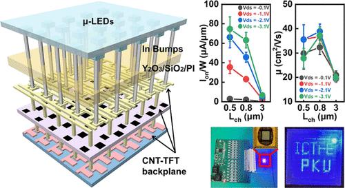
Micro-LED Microdisplays Driven by Carbon Nanotube Active-Matrix Backplanes
Micro-light-emitting-diodes (μLEDs) are poised to revolutionize flat-panel display (FPD) technology with their exceptional brightness, contrast ratio, energy efficiency, and ultrahigh resolutions, making them indispensable for augmented reality (AR) and virtual reality (VR) microdisplays. However, the realization of high pixel-per-inch (PPI) μLED microdisplays demands advanced thin-film transistor (TFT) backplanes with robust driving capabilities. Presently, single-crystalline silicon CMOS dominates the industry for this application, but its nontransparent nature, wafer size limitations, and high fabrication cost restrict its scalability. Alternative technologies, including low-temperature polycrystalline silicon (LTPS) and metal oxide semiconductors, fail to deliver the required small device dimensions, driving performance, and stability. Two-dimensional transition metal dichalcogenides (TMDs) have shown potential, but their integration has faced challenges, such as complex transfer processes and limited scalability, resulting in only semiactive-matrix display demonstrations. Here, we present a prototype active-matrix (AM) μLED microdisplay driven by optimized carbon nanotube (CNT) TFTs with Al2O3/SiO2 gate dielectric stack and Y2O3/SiO2/polyimide passivation layers. Our CNT TFTs with a channel length (Lch) of 3 μm achieve a driving current of ∼10 μA/μm and a mobility of ∼27 cm2/(V·s), while scaling Lch to 0.5 μm enhances the driving current to ∼80 μA/μm and a mobility of ∼40 cm2/(V·s), surpassing most previously reported CNT TFTs for AM displays and enabling AM-μLED microdisplays with a PPI up to 3400. Moreover, a heterogeneous integration process ultilizing flip-chip eutectic bonding was developed to assemble μLED arrays onto CNT TFT backplanes, achieving a yield of ∼100% aided by the PI layer. Furthermore, CNT TFT-based two-transistor, one-capacitor (2T1C) pixel-driving circuits and peripheral control circuits were designed to support both pulse amplitude modulation (PAM) and pulse width modulation (PWM) of μLED operation. These advancements culminate in a 32 × 32-pixel AM-μLED prototype microdisplay with a PPI of 357, capable of dynamic image and video display. Our work demonstrates CNT TFTs as a viable and scalable solution for next-generation μLED microdisplays.
期刊介绍:
ACS Nano, published monthly, serves as an international forum for comprehensive articles on nanoscience and nanotechnology research at the intersections of chemistry, biology, materials science, physics, and engineering. The journal fosters communication among scientists in these communities, facilitating collaboration, new research opportunities, and advancements through discoveries. ACS Nano covers synthesis, assembly, characterization, theory, and simulation of nanostructures, nanobiotechnology, nanofabrication, methods and tools for nanoscience and nanotechnology, and self- and directed-assembly. Alongside original research articles, it offers thorough reviews, perspectives on cutting-edge research, and discussions envisioning the future of nanoscience and nanotechnology.


 求助内容:
求助内容: 应助结果提醒方式:


