利用三维柔性探头对微尺度发光二极管晶圆进行电致发光测量
IF 40.9
1区 工程技术
Q1 ENGINEERING, ELECTRICAL & ELECTRONIC
引用次数: 0
摘要
微型发光二极管(led)可以用作下一代显示器的背光。然而,高密度、大面积的显示器在制造产量方面有严格的要求,并且缺乏有效的工具——能够进行高通量电致发光检测,这可以促进已知的好模转移印刷——限制了微型led的大规模生产。在这里,我们展示了一个三维柔性探头(类似于半导体测试中用于晶圆级芯片测试的刚性探头卡)和相应的电致发光检测系统可以测量微尺度led的电学和光学特性,而不会引入表面缺陷。探头中的弹性微柱可以自适应变形以匹配微型LED的表面形态,并且可以容忍LED衬垫之间的高度差异。探头头有32 × 32对探头,可以在0.5秒内使用无源矩阵驱动方法同时测量1024个微型led。从探头到微型led的接触应力为0.91 MPa,比通常会产生表面缺陷的屈服应力至少低两个数量级。我们表明,该系统可以执行超过100万次的重复接触测量,而探头磨损可以忽略不计。本文章由计算机程序翻译,如有差异,请以英文原文为准。


Electroluminescence measurement of microscale light-emitting diode wafers using a three-dimensional flexible probe head
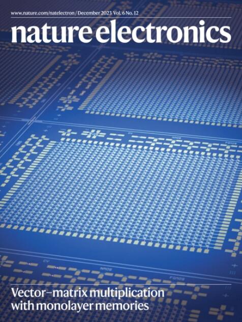
Microscale light-emitting diodes (LEDs) could be used as the backlights of next-generation displays. However, high-density, large-area displays have stringent requirements in terms of manufacturing yields and the lack of effective tools—capable of high-throughput electroluminescence detection, which can facilitate known-good-die transfer printing—limits mass production of microscale LEDs. Here we show that a three-dimensional flexible probe head (analogous to the rigid probe cards used to conduct wafer-level tests of chips in semiconducting testing) and a corresponding electroluminescence detection system can measure the electrical and optical properties of microscale LEDs without introducing surface defects. Elastic microposts in the probe head can deform adaptively to match the surface morphology of the microscale LEDs and can tolerate height differences between the LED pads. The probe head has 32 × 32 pairs of probes that can simultaneously measure 1,024 microscale LEDs using a passive-matrix driving approach in 0.5 s. The contact stress applied from the probe head to the microscale LEDs is 0.91 MPa, which is at least two orders of magnitude lower than the yield stress that will typically create surface defects. We show that the system can perform more than 1 million repeated contact measurements with negligible probe wear. High-throughput and reversible characterization of microscale light-emitting diode wafers can be performed using a flexible probe head containing arrays of elastomer microposts, which reduce surface defects and probe wear.
求助全文
通过发布文献求助,成功后即可免费获取论文全文。
去求助
来源期刊

Nature Electronics
Engineering-Electrical and Electronic Engineering
CiteScore
47.50
自引率
2.30%
发文量
159
期刊介绍:
Nature Electronics is a comprehensive journal that publishes both fundamental and applied research in the field of electronics. It encompasses a wide range of topics, including the study of new phenomena and devices, the design and construction of electronic circuits, and the practical applications of electronics. In addition, the journal explores the commercial and industrial aspects of electronics research.
The primary focus of Nature Electronics is on the development of technology and its potential impact on society. The journal incorporates the contributions of scientists, engineers, and industry professionals, offering a platform for their research findings. Moreover, Nature Electronics provides insightful commentary, thorough reviews, and analysis of the key issues that shape the field, as well as the technologies that are reshaping society.
Like all journals within the prestigious Nature brand, Nature Electronics upholds the highest standards of quality. It maintains a dedicated team of professional editors and follows a fair and rigorous peer-review process. The journal also ensures impeccable copy-editing and production, enabling swift publication. Additionally, Nature Electronics prides itself on its editorial independence, ensuring unbiased and impartial reporting.
In summary, Nature Electronics is a leading journal that publishes cutting-edge research in electronics. With its multidisciplinary approach and commitment to excellence, the journal serves as a valuable resource for scientists, engineers, and industry professionals seeking to stay at the forefront of advancements in the field.
 求助内容:
求助内容: 应助结果提醒方式:


