静电纳米掩模在铁电薄膜中形成180°畴壁

IF 12.5 1区 综合性期刊 Q1 MULTIDISCIPLINARY SCIENCES
Xiangbin Cai, Yueze Tan, Chao Chen, Changsheng Chen, Xiangli Che, Chao Xu, Yan Zhao, Haiyang Pan, Yaoding Lou, Jefferson Zhe Liu, Jesús Zúñiga Pérez, Weibo Gao, Long-Qing Chen, Jun-Ming Liu, Deyang Chen, Ye Zhu
{"title":"静电纳米掩模在铁电薄膜中形成180°畴壁","authors":"Xiangbin Cai,&nbsp;Yueze Tan,&nbsp;Chao Chen,&nbsp;Changsheng Chen,&nbsp;Xiangli Che,&nbsp;Chao Xu,&nbsp;Yan Zhao,&nbsp;Haiyang Pan,&nbsp;Yaoding Lou,&nbsp;Jefferson Zhe Liu,&nbsp;Jesús Zúñiga Pérez,&nbsp;Weibo Gao,&nbsp;Long-Qing Chen,&nbsp;Jun-Ming Liu,&nbsp;Deyang Chen,&nbsp;Ye Zhu","doi":"10.1126/sciadv.adv9194","DOIUrl":null,"url":null,"abstract":"<div >Ferroelectric domain walls (FDWs) exhibit exotic structural and electronic properties, positioning them as a promising functional element for next-generation nanoelectronics. However, achieving the deterministic creation of FDWs with nanoscale precision and controlled polarization of domains remains a substantial challenge for the scalable FDW-device fabrication and circuit design. Here, we demonstrate a strategy for FDW engineering by tailoring the interfacial electrostatic profile. Using SrRuO<sub>3</sub> islands as “nano-masks,” we spatially modulate the interfacial atomic termination to generate alternating positive and negative built-in electric fields. The boundaries where the electric field switches polarity drive the formation of 180° FDWs in BiFeO<sub>3</sub> thin films. This mechanism is validated through theoretical calculations and direct experimental observations. Furthermore, atomic-scale analysis reveals localized lattice distortions, structural chirality of the FDWs, as well as the edge effect of SrRuO<sub>3</sub> islands on the position precision of FDW nucleation. Our findings pave the way toward a scalable and controllable bottom-up FDW-growth technique for future FDW nanoelectronics.</div>","PeriodicalId":21609,"journal":{"name":"Science Advances","volume":"11 24","pages":""},"PeriodicalIF":12.5000,"publicationDate":"2025-06-11","publicationTypes":"Journal Article","fieldsOfStudy":null,"isOpenAccess":false,"openAccessPdf":"https://www.science.org/doi/reader/10.1126/sciadv.adv9194","citationCount":"0","resultStr":"{\"title\":\"Electrostatic nano-mask patterned 180° domain walls in a ferroelectric film\",\"authors\":\"Xiangbin Cai,&nbsp;Yueze Tan,&nbsp;Chao Chen,&nbsp;Changsheng Chen,&nbsp;Xiangli Che,&nbsp;Chao Xu,&nbsp;Yan Zhao,&nbsp;Haiyang Pan,&nbsp;Yaoding Lou,&nbsp;Jefferson Zhe Liu,&nbsp;Jesús Zúñiga Pérez,&nbsp;Weibo Gao,&nbsp;Long-Qing Chen,&nbsp;Jun-Ming Liu,&nbsp;Deyang Chen,&nbsp;Ye Zhu\",\"doi\":\"10.1126/sciadv.adv9194\",\"DOIUrl\":null,\"url\":null,\"abstract\":\"<div >Ferroelectric domain walls (FDWs) exhibit exotic structural and electronic properties, positioning them as a promising functional element for next-generation nanoelectronics. However, achieving the deterministic creation of FDWs with nanoscale precision and controlled polarization of domains remains a substantial challenge for the scalable FDW-device fabrication and circuit design. Here, we demonstrate a strategy for FDW engineering by tailoring the interfacial electrostatic profile. Using SrRuO<sub>3</sub> islands as “nano-masks,” we spatially modulate the interfacial atomic termination to generate alternating positive and negative built-in electric fields. The boundaries where the electric field switches polarity drive the formation of 180° FDWs in BiFeO<sub>3</sub> thin films. This mechanism is validated through theoretical calculations and direct experimental observations. Furthermore, atomic-scale analysis reveals localized lattice distortions, structural chirality of the FDWs, as well as the edge effect of SrRuO<sub>3</sub> islands on the position precision of FDW nucleation. Our findings pave the way toward a scalable and controllable bottom-up FDW-growth technique for future FDW nanoelectronics.</div>\",\"PeriodicalId\":21609,\"journal\":{\"name\":\"Science Advances\",\"volume\":\"11 24\",\"pages\":\"\"},\"PeriodicalIF\":12.5000,\"publicationDate\":\"2025-06-11\",\"publicationTypes\":\"Journal Article\",\"fieldsOfStudy\":null,\"isOpenAccess\":false,\"openAccessPdf\":\"https://www.science.org/doi/reader/10.1126/sciadv.adv9194\",\"citationCount\":\"0\",\"resultStr\":null,\"platform\":\"Semanticscholar\",\"paperid\":null,\"PeriodicalName\":\"Science Advances\",\"FirstCategoryId\":\"103\",\"ListUrlMain\":\"https://www.science.org/doi/10.1126/sciadv.adv9194\",\"RegionNum\":1,\"RegionCategory\":\"综合性期刊\",\"ArticlePicture\":[],\"TitleCN\":null,\"AbstractTextCN\":null,\"PMCID\":null,\"EPubDate\":\"\",\"PubModel\":\"\",\"JCR\":\"Q1\",\"JCRName\":\"MULTIDISCIPLINARY SCIENCES\",\"Score\":null,\"Total\":0}","platform":"Semanticscholar","paperid":null,"PeriodicalName":"Science Advances","FirstCategoryId":"103","ListUrlMain":"https://www.science.org/doi/10.1126/sciadv.adv9194","RegionNum":1,"RegionCategory":"综合性期刊","ArticlePicture":[],"TitleCN":null,"AbstractTextCN":null,"PMCID":null,"EPubDate":"","PubModel":"","JCR":"Q1","JCRName":"MULTIDISCIPLINARY SCIENCES","Score":null,"Total":0}
引用次数: 0

摘要

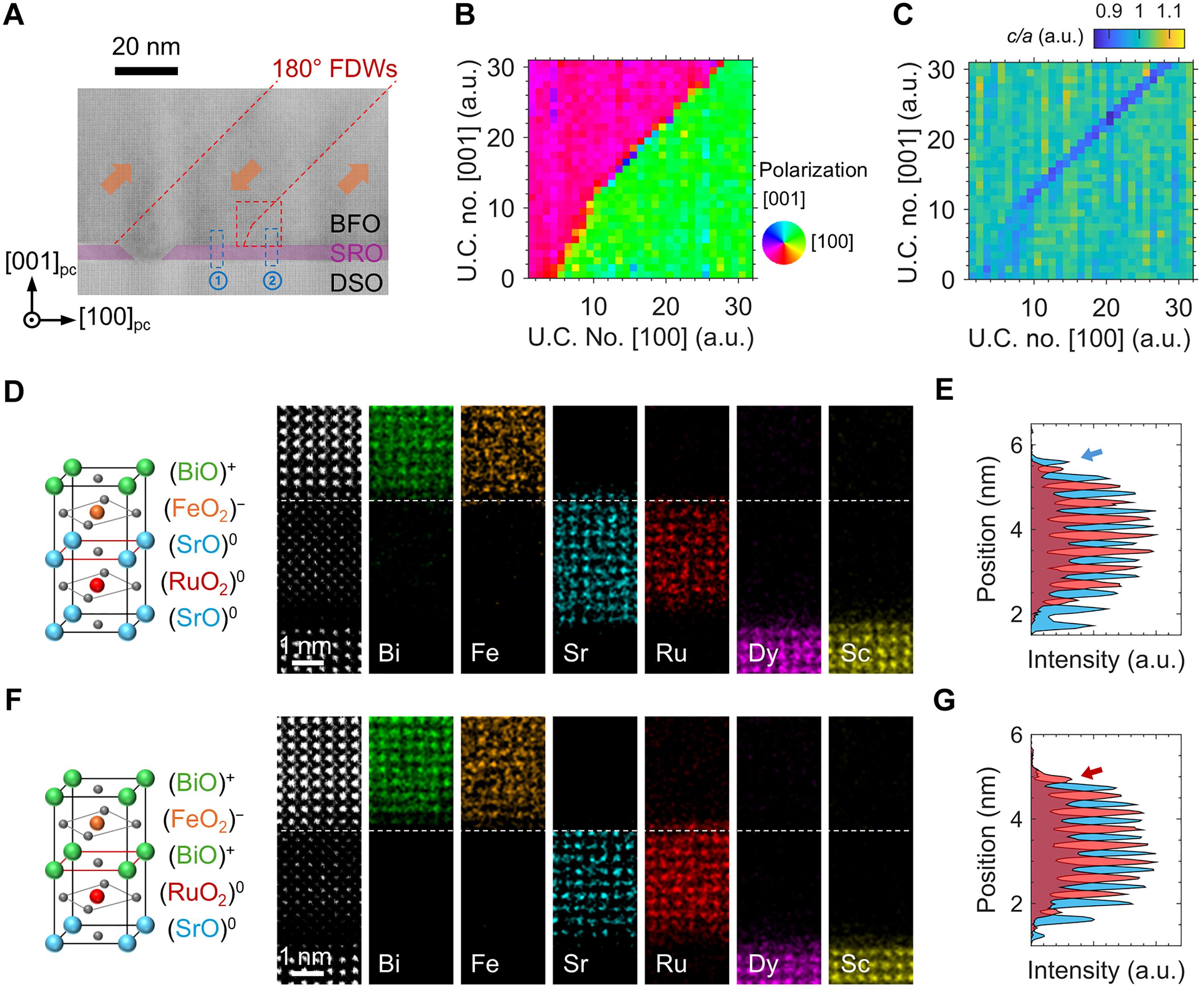
铁电畴壁(FDWs)表现出独特的结构和电子特性,使其成为下一代纳米电子学中有前途的功能元件。然而,实现纳米级精度和可控极化域的fdw的确定性创建仍然是可扩展fdw器件制造和电路设计的重大挑战。在这里,我们展示了一种通过调整界面静电剖面来实现FDW工程的策略。使用srruo3岛作为“纳米掩模”,我们在空间上调节界面原子端部,以产生交替的正负内置电场。电场切换极性的边界驱动bifeo3薄膜中180°FDWs的形成。这一机制通过理论计算和直接实验观察得到了验证。此外,原子尺度分析揭示了FDW的局域晶格畸变、结构手性以及srruo3岛的边缘效应对FDW成核位置精度的影响。我们的发现为未来FDW纳米电子学的可扩展和可控的自下而上的FDW生长技术铺平了道路。
本文章由计算机程序翻译,如有差异,请以英文原文为准。

Electrostatic nano-mask patterned 180° domain walls in a ferroelectric film

Electrostatic nano-mask patterned 180° domain walls in a ferroelectric film
Ferroelectric domain walls (FDWs) exhibit exotic structural and electronic properties, positioning them as a promising functional element for next-generation nanoelectronics. However, achieving the deterministic creation of FDWs with nanoscale precision and controlled polarization of domains remains a substantial challenge for the scalable FDW-device fabrication and circuit design. Here, we demonstrate a strategy for FDW engineering by tailoring the interfacial electrostatic profile. Using SrRuO3 islands as “nano-masks,” we spatially modulate the interfacial atomic termination to generate alternating positive and negative built-in electric fields. The boundaries where the electric field switches polarity drive the formation of 180° FDWs in BiFeO3 thin films. This mechanism is validated through theoretical calculations and direct experimental observations. Furthermore, atomic-scale analysis reveals localized lattice distortions, structural chirality of the FDWs, as well as the edge effect of SrRuO3 islands on the position precision of FDW nucleation. Our findings pave the way toward a scalable and controllable bottom-up FDW-growth technique for future FDW nanoelectronics.
求助全文
通过发布文献求助,成功后即可免费获取论文全文。 去求助
来源期刊
Science Advances
Science Advances 综合性期刊-综合性期刊
CiteScore
21.40
自引率
1.50%
发文量
1937
审稿时长
29 weeks
期刊介绍: Science Advances, an open-access journal by AAAS, publishes impactful research in diverse scientific areas. It aims for fair, fast, and expert peer review, providing freely accessible research to readers. Led by distinguished scientists, the journal supports AAAS's mission by extending Science magazine's capacity to identify and promote significant advances. Evolving digital publishing technologies play a crucial role in advancing AAAS's global mission for science communication and benefitting humankind.
×
引用
GB/T 7714-2015
复制
MLA
复制
APA
复制
导出至
BibTeX EndNote RefMan NoteFirst NoteExpress
×
提示
您的信息不完整,为了账户安全,请先补充。
现在去补充
×
提示
您因"违规操作"
具体请查看互助需知
我知道了
×
提示
确定
请完成安全验证×
copy
已复制链接
快去分享给好友吧!
我知道了
右上角分享
点击右上角分享
0
联系我们:info@booksci.cn Book学术提供免费学术资源搜索服务,方便国内外学者检索中英文文献。致力于提供最便捷和优质的服务体验。 Copyright © 2023 布克学术 All rights reserved.
京ICP备2023020795号-1
ghs 京公网安备 11010802042870号
Book学术文献互助
Book学术文献互助群
群 号:604180095
Book学术官方微信