Wenda Zhang, Xijian Duan, Lei Chen, Kai Wang, Yujie Song*, Weigao Wang* and Xiao Wei Sun*,
{"title":"发光二极管用高频刻蚀法合成深蓝InP量子点","authors":"Wenda Zhang, Xijian Duan, Lei Chen, Kai Wang, Yujie Song*, Weigao Wang* and Xiao Wei Sun*, ","doi":"10.1021/acsaelm.5c0050310.1021/acsaelm.5c00503","DOIUrl":null,"url":null,"abstract":"<p >Red, green, and sky-blue InP quantum dots (QDs) are currently bridging the gap with CdSe-based QDs in terms of the photoluminescence quantum yields (PLQY). However, the sensitivity of InP QDs to water and oxygen, coupled with the increased specific surface area of smaller pure-blue and deep-blue QDs, leads to diminished PLQY, consequently restricting the fabrication of highly efficient blue InP quantum dot light-emitting diodes (QLEDs). Here, high-temperature nucleation is utilized to produce highly crystalline InP cores, followed by low-temperature HF etching. This dual-treatment method simultaneously addresses surface phosphate defects and diminishes QD size, ultimately yielding pure-blue InP QDs with a PLQY of 73% at 466 nm and deep-blue InP QDs with a PLQY of 52% at 451 nm. Notably, by fine-tuning the HF dosage, 421 nm deep-blue InP QDs, representing the shortest wavelength to date, were successfully prepared. Additionally, enhancing carrier injection efficiency was achieved by replacing long-chain 1-dodecanethiol (DDT) ligands with short-chain 1-octanethiol (OT) ligands through ligand exchange. QLEDs exhibited an external quantum efficiency of 0.8% with an emission wavelength of 468 nm, providing a perspective for the fabrication of InP blue QLEDs via this etching technique.</p>","PeriodicalId":3,"journal":{"name":"ACS Applied Electronic Materials","volume":"7 11","pages":"5061–5068 5061–5068"},"PeriodicalIF":4.7000,"publicationDate":"2025-05-05","publicationTypes":"Journal Article","fieldsOfStudy":null,"isOpenAccess":false,"openAccessPdf":"","citationCount":"0","resultStr":"{\"title\":\"Synthesis of Deep Blue InP Quantum Dots via HF Etching for Light-Emitting Diodes\",\"authors\":\"Wenda Zhang, Xijian Duan, Lei Chen, Kai Wang, Yujie Song*, Weigao Wang* and Xiao Wei Sun*, \",\"doi\":\"10.1021/acsaelm.5c0050310.1021/acsaelm.5c00503\",\"DOIUrl\":null,\"url\":null,\"abstract\":\"<p >Red, green, and sky-blue InP quantum dots (QDs) are currently bridging the gap with CdSe-based QDs in terms of the photoluminescence quantum yields (PLQY). However, the sensitivity of InP QDs to water and oxygen, coupled with the increased specific surface area of smaller pure-blue and deep-blue QDs, leads to diminished PLQY, consequently restricting the fabrication of highly efficient blue InP quantum dot light-emitting diodes (QLEDs). Here, high-temperature nucleation is utilized to produce highly crystalline InP cores, followed by low-temperature HF etching. This dual-treatment method simultaneously addresses surface phosphate defects and diminishes QD size, ultimately yielding pure-blue InP QDs with a PLQY of 73% at 466 nm and deep-blue InP QDs with a PLQY of 52% at 451 nm. Notably, by fine-tuning the HF dosage, 421 nm deep-blue InP QDs, representing the shortest wavelength to date, were successfully prepared. Additionally, enhancing carrier injection efficiency was achieved by replacing long-chain 1-dodecanethiol (DDT) ligands with short-chain 1-octanethiol (OT) ligands through ligand exchange. QLEDs exhibited an external quantum efficiency of 0.8% with an emission wavelength of 468 nm, providing a perspective for the fabrication of InP blue QLEDs via this etching technique.</p>\",\"PeriodicalId\":3,\"journal\":{\"name\":\"ACS Applied Electronic Materials\",\"volume\":\"7 11\",\"pages\":\"5061–5068 5061–5068\"},\"PeriodicalIF\":4.7000,\"publicationDate\":\"2025-05-05\",\"publicationTypes\":\"Journal Article\",\"fieldsOfStudy\":null,\"isOpenAccess\":false,\"openAccessPdf\":\"\",\"citationCount\":\"0\",\"resultStr\":null,\"platform\":\"Semanticscholar\",\"paperid\":null,\"PeriodicalName\":\"ACS Applied Electronic Materials\",\"FirstCategoryId\":\"88\",\"ListUrlMain\":\"https://pubs.acs.org/doi/10.1021/acsaelm.5c00503\",\"RegionNum\":3,\"RegionCategory\":\"材料科学\",\"ArticlePicture\":[],\"TitleCN\":null,\"AbstractTextCN\":null,\"PMCID\":null,\"EPubDate\":\"\",\"PubModel\":\"\",\"JCR\":\"Q1\",\"JCRName\":\"ENGINEERING, ELECTRICAL & ELECTRONIC\",\"Score\":null,\"Total\":0}","platform":"Semanticscholar","paperid":null,"PeriodicalName":"ACS Applied Electronic Materials","FirstCategoryId":"88","ListUrlMain":"https://pubs.acs.org/doi/10.1021/acsaelm.5c00503","RegionNum":3,"RegionCategory":"材料科学","ArticlePicture":[],"TitleCN":null,"AbstractTextCN":null,"PMCID":null,"EPubDate":"","PubModel":"","JCR":"Q1","JCRName":"ENGINEERING, ELECTRICAL & ELECTRONIC","Score":null,"Total":0}
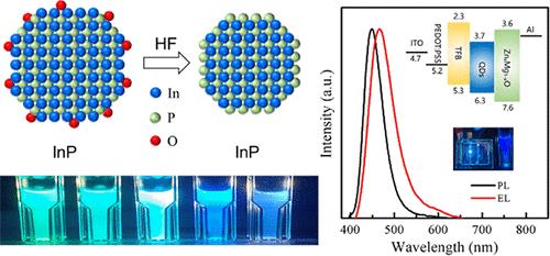
Synthesis of Deep Blue InP Quantum Dots via HF Etching for Light-Emitting Diodes
Red, green, and sky-blue InP quantum dots (QDs) are currently bridging the gap with CdSe-based QDs in terms of the photoluminescence quantum yields (PLQY). However, the sensitivity of InP QDs to water and oxygen, coupled with the increased specific surface area of smaller pure-blue and deep-blue QDs, leads to diminished PLQY, consequently restricting the fabrication of highly efficient blue InP quantum dot light-emitting diodes (QLEDs). Here, high-temperature nucleation is utilized to produce highly crystalline InP cores, followed by low-temperature HF etching. This dual-treatment method simultaneously addresses surface phosphate defects and diminishes QD size, ultimately yielding pure-blue InP QDs with a PLQY of 73% at 466 nm and deep-blue InP QDs with a PLQY of 52% at 451 nm. Notably, by fine-tuning the HF dosage, 421 nm deep-blue InP QDs, representing the shortest wavelength to date, were successfully prepared. Additionally, enhancing carrier injection efficiency was achieved by replacing long-chain 1-dodecanethiol (DDT) ligands with short-chain 1-octanethiol (OT) ligands through ligand exchange. QLEDs exhibited an external quantum efficiency of 0.8% with an emission wavelength of 468 nm, providing a perspective for the fabrication of InP blue QLEDs via this etching technique.
期刊介绍:
ACS Applied Electronic Materials is an interdisciplinary journal publishing original research covering all aspects of electronic materials. The journal is devoted to reports of new and original experimental and theoretical research of an applied nature that integrate knowledge in the areas of materials science, engineering, optics, physics, and chemistry into important applications of electronic materials. Sample research topics that span the journal's scope are inorganic, organic, ionic and polymeric materials with properties that include conducting, semiconducting, superconducting, insulating, dielectric, magnetic, optoelectronic, piezoelectric, ferroelectric and thermoelectric.
Indexed/Abstracted:
Web of Science SCIE
Scopus
CAS
INSPEC
Portico

 求助内容:
求助内容: 应助结果提醒方式:


