{"title":"具有宽带隙薄膜氧化物异质结的空间电荷限制肖特基二极管","authors":"Jihun Lim*, ","doi":"10.1021/acsaelm.5c0008310.1021/acsaelm.5c00083","DOIUrl":null,"url":null,"abstract":"<p >Noncrystalline thin-film Schottky diodes are cost-effective but often exhibit unreliable electrical characteristics due to material imperfections. In this work, a Schottky diode structure is presented utilizing in situ grown Ta<sub>2</sub>O<sub>5</sub> and ZnO thin films deposited at room temperature. The low conduction band offset across the interface of the heterogeneous oxides facilitates efficient electron injection under forward bias. Capacitance–voltage characterization reveals a robust Schottky barrier at the Au/Ta<sub>2</sub>O<sub>5</sub> interface without a significant barrier thinning effect, enabling high-voltage breakdown up to 65 V and a high on/off ratio of 1 × 10<sup>8</sup>. In demonstrations, the thin-film structure shows Schottky contact characteristics using even a relatively low work function metal of ITO, allowing the operation of transparent Schottky diodes. The diodes show additional potential for applications, including RF-to-DC conversion leveraging space charge capacitance at the Ta<sub>2</sub>O<sub>5</sub>/ZnO junction and rectifying resistive random access memory devices. This work highlights a promising approach for integrating low-cost, high-reliability Schottky diodes into back-end-of-line processes for wireless electronics and power devices.</p>","PeriodicalId":3,"journal":{"name":"ACS Applied Electronic Materials","volume":"7 11","pages":"4755–4762 4755–4762"},"PeriodicalIF":4.7000,"publicationDate":"2025-05-20","publicationTypes":"Journal Article","fieldsOfStudy":null,"isOpenAccess":false,"openAccessPdf":"","citationCount":"0","resultStr":"{\"title\":\"Space-Charge Limited Schottky Diodes with Wide-Bandgap Thin-Film Oxide Heterojunctions\",\"authors\":\"Jihun Lim*, \",\"doi\":\"10.1021/acsaelm.5c0008310.1021/acsaelm.5c00083\",\"DOIUrl\":null,\"url\":null,\"abstract\":\"<p >Noncrystalline thin-film Schottky diodes are cost-effective but often exhibit unreliable electrical characteristics due to material imperfections. In this work, a Schottky diode structure is presented utilizing in situ grown Ta<sub>2</sub>O<sub>5</sub> and ZnO thin films deposited at room temperature. The low conduction band offset across the interface of the heterogeneous oxides facilitates efficient electron injection under forward bias. Capacitance–voltage characterization reveals a robust Schottky barrier at the Au/Ta<sub>2</sub>O<sub>5</sub> interface without a significant barrier thinning effect, enabling high-voltage breakdown up to 65 V and a high on/off ratio of 1 × 10<sup>8</sup>. In demonstrations, the thin-film structure shows Schottky contact characteristics using even a relatively low work function metal of ITO, allowing the operation of transparent Schottky diodes. The diodes show additional potential for applications, including RF-to-DC conversion leveraging space charge capacitance at the Ta<sub>2</sub>O<sub>5</sub>/ZnO junction and rectifying resistive random access memory devices. This work highlights a promising approach for integrating low-cost, high-reliability Schottky diodes into back-end-of-line processes for wireless electronics and power devices.</p>\",\"PeriodicalId\":3,\"journal\":{\"name\":\"ACS Applied Electronic Materials\",\"volume\":\"7 11\",\"pages\":\"4755–4762 4755–4762\"},\"PeriodicalIF\":4.7000,\"publicationDate\":\"2025-05-20\",\"publicationTypes\":\"Journal Article\",\"fieldsOfStudy\":null,\"isOpenAccess\":false,\"openAccessPdf\":\"\",\"citationCount\":\"0\",\"resultStr\":null,\"platform\":\"Semanticscholar\",\"paperid\":null,\"PeriodicalName\":\"ACS Applied Electronic Materials\",\"FirstCategoryId\":\"88\",\"ListUrlMain\":\"https://pubs.acs.org/doi/10.1021/acsaelm.5c00083\",\"RegionNum\":3,\"RegionCategory\":\"材料科学\",\"ArticlePicture\":[],\"TitleCN\":null,\"AbstractTextCN\":null,\"PMCID\":null,\"EPubDate\":\"\",\"PubModel\":\"\",\"JCR\":\"Q1\",\"JCRName\":\"ENGINEERING, ELECTRICAL & ELECTRONIC\",\"Score\":null,\"Total\":0}","platform":"Semanticscholar","paperid":null,"PeriodicalName":"ACS Applied Electronic Materials","FirstCategoryId":"88","ListUrlMain":"https://pubs.acs.org/doi/10.1021/acsaelm.5c00083","RegionNum":3,"RegionCategory":"材料科学","ArticlePicture":[],"TitleCN":null,"AbstractTextCN":null,"PMCID":null,"EPubDate":"","PubModel":"","JCR":"Q1","JCRName":"ENGINEERING, ELECTRICAL & ELECTRONIC","Score":null,"Total":0}
Space-Charge Limited Schottky Diodes with Wide-Bandgap Thin-Film Oxide Heterojunctions
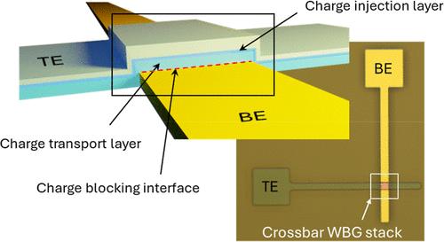
Noncrystalline thin-film Schottky diodes are cost-effective but often exhibit unreliable electrical characteristics due to material imperfections. In this work, a Schottky diode structure is presented utilizing in situ grown Ta2O5 and ZnO thin films deposited at room temperature. The low conduction band offset across the interface of the heterogeneous oxides facilitates efficient electron injection under forward bias. Capacitance–voltage characterization reveals a robust Schottky barrier at the Au/Ta2O5 interface without a significant barrier thinning effect, enabling high-voltage breakdown up to 65 V and a high on/off ratio of 1 × 10⁸. In demonstrations, the thin-film structure shows Schottky contact characteristics using even a relatively low work function metal of ITO, allowing the operation of transparent Schottky diodes. The diodes show additional potential for applications, including RF-to-DC conversion leveraging space charge capacitance at the Ta2O5/ZnO junction and rectifying resistive random access memory devices. This work highlights a promising approach for integrating low-cost, high-reliability Schottky diodes into back-end-of-line processes for wireless electronics and power devices.
期刊介绍:
ACS Applied Electronic Materials is an interdisciplinary journal publishing original research covering all aspects of electronic materials. The journal is devoted to reports of new and original experimental and theoretical research of an applied nature that integrate knowledge in the areas of materials science, engineering, optics, physics, and chemistry into important applications of electronic materials. Sample research topics that span the journal's scope are inorganic, organic, ionic and polymeric materials with properties that include conducting, semiconducting, superconducting, insulating, dielectric, magnetic, optoelectronic, piezoelectric, ferroelectric and thermoelectric.
Indexed/Abstracted:
Web of Science SCIE
Scopus
CAS
INSPEC
Portico

 求助内容:
求助内容: 应助结果提醒方式:


