Carlos Nunez Lobato, Vincenzo Esposito, Nini Pryds and Dennis V. Christensen*,
{"title":"硅平台上导电SrTiO3薄膜的生长研究","authors":"Carlos Nunez Lobato, Vincenzo Esposito, Nini Pryds and Dennis V. Christensen*, ","doi":"10.1021/acsaelm.4c0218310.1021/acsaelm.4c02183","DOIUrl":null,"url":null,"abstract":"<p >The challenge of interfacing complex oxides with silicon has restricted their practical use in scalable oxide-based electronic devices. The growth of prototypical perovskite SrTiO<sub>3</sub> via molecular beam epitaxy has enabled commercially available SrTiO<sub>3</sub>/Si substrates, which can serve as a growth template for silicon-integrated complex oxides deposited using other techniques. Here, we deposit conductive Nb-doped SrTiO<sub>3</sub> (NSTO) thin films with pulsed laser deposition on commercial SrTiO<sub>3</sub>/Si substrates and compare the structural and electronic characteristics with NSTO deposited on perovskite single crystal (LaAlO<sub>3</sub>)<sub>0.3</sub>(Sr<sub>2</sub>TaAlO<sub>6</sub>)<sub>0.7</sub> (LSAT) as well as crystalline silicon terminated with SiO<sub>2</sub> or amorphous Si<sub>3</sub>N<sub>4</sub>. We find that NSTO thin films deposited on LSAT and SrTiO<sub>3</sub>/Si both result in epitaxial films with similar conductivity but with the lattice mismatch resulting in a biaxial compressive strain of −1.6% on LSAT, whereas the difference in thermal expansion coefficients between NSTO and SrTiO<sub>3</sub>/Si induces a biaxial tensile strain of +0.4%. In contrast, NSTO deposited on Si<sub>3</sub>N<sub>4</sub>/Si or SiO<sub>2</sub>/Si exhibit a mosaic-granular structure, where the conductive performance deteriorates drastically as the film thickness falls below the average grain size of the film (<30–50 nm). Our findings underscore the achievement of both superior epitaxial and transport characteristics in films grown on commercial SrTiO<sub>3</sub>/Si substrates compared to other silicon platforms, as well as advancing the successful integration of multifunctional oxides on silicon.</p>","PeriodicalId":3,"journal":{"name":"ACS Applied Electronic Materials","volume":"7 11","pages":"4729–4737 4729–4737"},"PeriodicalIF":4.7000,"publicationDate":"2025-05-21","publicationTypes":"Journal Article","fieldsOfStudy":null,"isOpenAccess":false,"openAccessPdf":"","citationCount":"0","resultStr":"{\"title\":\"A Growth Study of Conductive SrTiO3 Thin Films on Silicon Platforms\",\"authors\":\"Carlos Nunez Lobato, Vincenzo Esposito, Nini Pryds and Dennis V. Christensen*, \",\"doi\":\"10.1021/acsaelm.4c0218310.1021/acsaelm.4c02183\",\"DOIUrl\":null,\"url\":null,\"abstract\":\"<p >The challenge of interfacing complex oxides with silicon has restricted their practical use in scalable oxide-based electronic devices. The growth of prototypical perovskite SrTiO<sub>3</sub> via molecular beam epitaxy has enabled commercially available SrTiO<sub>3</sub>/Si substrates, which can serve as a growth template for silicon-integrated complex oxides deposited using other techniques. Here, we deposit conductive Nb-doped SrTiO<sub>3</sub> (NSTO) thin films with pulsed laser deposition on commercial SrTiO<sub>3</sub>/Si substrates and compare the structural and electronic characteristics with NSTO deposited on perovskite single crystal (LaAlO<sub>3</sub>)<sub>0.3</sub>(Sr<sub>2</sub>TaAlO<sub>6</sub>)<sub>0.7</sub> (LSAT) as well as crystalline silicon terminated with SiO<sub>2</sub> or amorphous Si<sub>3</sub>N<sub>4</sub>. We find that NSTO thin films deposited on LSAT and SrTiO<sub>3</sub>/Si both result in epitaxial films with similar conductivity but with the lattice mismatch resulting in a biaxial compressive strain of −1.6% on LSAT, whereas the difference in thermal expansion coefficients between NSTO and SrTiO<sub>3</sub>/Si induces a biaxial tensile strain of +0.4%. In contrast, NSTO deposited on Si<sub>3</sub>N<sub>4</sub>/Si or SiO<sub>2</sub>/Si exhibit a mosaic-granular structure, where the conductive performance deteriorates drastically as the film thickness falls below the average grain size of the film (<30–50 nm). Our findings underscore the achievement of both superior epitaxial and transport characteristics in films grown on commercial SrTiO<sub>3</sub>/Si substrates compared to other silicon platforms, as well as advancing the successful integration of multifunctional oxides on silicon.</p>\",\"PeriodicalId\":3,\"journal\":{\"name\":\"ACS Applied Electronic Materials\",\"volume\":\"7 11\",\"pages\":\"4729–4737 4729–4737\"},\"PeriodicalIF\":4.7000,\"publicationDate\":\"2025-05-21\",\"publicationTypes\":\"Journal Article\",\"fieldsOfStudy\":null,\"isOpenAccess\":false,\"openAccessPdf\":\"\",\"citationCount\":\"0\",\"resultStr\":null,\"platform\":\"Semanticscholar\",\"paperid\":null,\"PeriodicalName\":\"ACS Applied Electronic Materials\",\"FirstCategoryId\":\"88\",\"ListUrlMain\":\"https://pubs.acs.org/doi/10.1021/acsaelm.4c02183\",\"RegionNum\":3,\"RegionCategory\":\"材料科学\",\"ArticlePicture\":[],\"TitleCN\":null,\"AbstractTextCN\":null,\"PMCID\":null,\"EPubDate\":\"\",\"PubModel\":\"\",\"JCR\":\"Q1\",\"JCRName\":\"ENGINEERING, ELECTRICAL & ELECTRONIC\",\"Score\":null,\"Total\":0}","platform":"Semanticscholar","paperid":null,"PeriodicalName":"ACS Applied Electronic Materials","FirstCategoryId":"88","ListUrlMain":"https://pubs.acs.org/doi/10.1021/acsaelm.4c02183","RegionNum":3,"RegionCategory":"材料科学","ArticlePicture":[],"TitleCN":null,"AbstractTextCN":null,"PMCID":null,"EPubDate":"","PubModel":"","JCR":"Q1","JCRName":"ENGINEERING, ELECTRICAL & ELECTRONIC","Score":null,"Total":0}
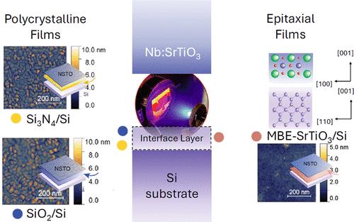
A Growth Study of Conductive SrTiO3 Thin Films on Silicon Platforms
The challenge of interfacing complex oxides with silicon has restricted their practical use in scalable oxide-based electronic devices. The growth of prototypical perovskite SrTiO3 via molecular beam epitaxy has enabled commercially available SrTiO3/Si substrates, which can serve as a growth template for silicon-integrated complex oxides deposited using other techniques. Here, we deposit conductive Nb-doped SrTiO3 (NSTO) thin films with pulsed laser deposition on commercial SrTiO3/Si substrates and compare the structural and electronic characteristics with NSTO deposited on perovskite single crystal (LaAlO3)0.3(Sr2TaAlO6)0.7 (LSAT) as well as crystalline silicon terminated with SiO2 or amorphous Si3N4. We find that NSTO thin films deposited on LSAT and SrTiO3/Si both result in epitaxial films with similar conductivity but with the lattice mismatch resulting in a biaxial compressive strain of −1.6% on LSAT, whereas the difference in thermal expansion coefficients between NSTO and SrTiO3/Si induces a biaxial tensile strain of +0.4%. In contrast, NSTO deposited on Si3N4/Si or SiO2/Si exhibit a mosaic-granular structure, where the conductive performance deteriorates drastically as the film thickness falls below the average grain size of the film (<30–50 nm). Our findings underscore the achievement of both superior epitaxial and transport characteristics in films grown on commercial SrTiO3/Si substrates compared to other silicon platforms, as well as advancing the successful integration of multifunctional oxides on silicon.
期刊介绍:
ACS Applied Electronic Materials is an interdisciplinary journal publishing original research covering all aspects of electronic materials. The journal is devoted to reports of new and original experimental and theoretical research of an applied nature that integrate knowledge in the areas of materials science, engineering, optics, physics, and chemistry into important applications of electronic materials. Sample research topics that span the journal's scope are inorganic, organic, ionic and polymeric materials with properties that include conducting, semiconducting, superconducting, insulating, dielectric, magnetic, optoelectronic, piezoelectric, ferroelectric and thermoelectric.
Indexed/Abstracted:
Web of Science SCIE
Scopus
CAS
INSPEC
Portico

 求助内容:
求助内容: 应助结果提醒方式:


