用于片上原型设计的排列多纳米线电路的柔性制造
IF 3.1
4区 工程技术
Q2 ENGINEERING, ELECTRICAL & ELECTRONIC
引用次数: 0
摘要
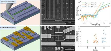
多个确定定位的半导体纳米线(NWs)电路是许多光子、量子或传统晶体管应用器件的基础。为了探索和迭代更大电路的设计,必须开发在目标位置快速放置和电气评估NWs的方法。我们提出并演示了在SiO2/Si衬底上构建多NW电路的概念,这使我们能够快速定位和定向NW组件到预先设计的配置中。在接触金属化之前,使用微操纵探针将NWs引导到具有期望设计的反应离子蚀刻沟槽中。定位工作在一个宽的组合沟的宽度和深度。定位精度取决于EBL模式,精确到±10纳米。为了演示这一概念,我们创建了具有各种特定方向的InP和InAs NWs电路。该概念用于迭代InP NW光电二极管的最佳触点创建过程。随后,我们可以在三个不同的样品上制造和电探测54个完全可操作的纳米光电二极管,从中可以获得二极管性能的可观统计数据。制造步骤与传统的Si CMOS结构直接兼容,应该适用于广泛的NW类型。精确度和放置率与高制造产量相结合,使复杂电路的概念原型验证成为可能。本文章由计算机程序翻译,如有差异,请以英文原文为准。
Flexible fabrication of aligned multi-nanowire circuits for on-chip prototyping
Circuits of multiple deterministically positioned semiconductor nanowires (NWs) is the basis of many devices for photonic, quantum, or conventional transistor applications. To explore and iterate on the design of larger circuits, the means to quickly place and electrically evaluate NWs at target locations must be developed. We propose and demonstrate a multi-NW circuit building concept on SiO2/Si substrates, which enables us to quickly position and orient NW components into pre-designed configurations. Micro-manipulator probes are used to guide the NWs into reactive ion etched trenches, with desired designs, before contact metallization. The positioning works over a wide combination of trench widths and depths. Positioning accuracies are contingent on EBL patterning, precise up to ±10 nm. To demonstrate the concept, we create circuits of InP and InAs NWs with a wide variety of specific orientations. The concept was used to iterate a procedure for creating optimal contacts for InP NW photodiodes. Subsequently, we could fabricate and electrically probe 54 fully operational nano-photodiodes placed on three different samples, from which considerable statistics of diode performance could be obtained. Fabrication steps are directly compatible with conventional Si CMOS architecture and should function for a wide range of NW types. The accuracy and rate of placement combined with high fabrication yields enables proof-of-concept prototyping of complex circuits.
求助全文
通过发布文献求助,成功后即可免费获取论文全文。
去求助
来源期刊

Microelectronic Engineering
工程技术-工程:电子与电气
CiteScore
5.30
自引率
4.30%
发文量
131
审稿时长
29 days
期刊介绍:
Microelectronic Engineering is the premier nanoprocessing, and nanotechnology journal focusing on fabrication of electronic, photonic, bioelectronic, electromechanic and fluidic devices and systems, and their applications in the broad areas of electronics, photonics, energy, life sciences, and environment. It covers also the expanding interdisciplinary field of "more than Moore" and "beyond Moore" integrated nanoelectronics / photonics and micro-/nano-/bio-systems. Through its unique mixture of peer-reviewed articles, reviews, accelerated publications, short and Technical notes, and the latest research news on key developments, Microelectronic Engineering provides comprehensive coverage of this exciting, interdisciplinary and dynamic new field for researchers in academia and professionals in industry.
 求助内容:
求助内容: 应助结果提醒方式:


