Li Li , Zhengjin Weng , Qianqian Wu , Jialing Jian , Liangliang Lin , Xiaofeng Gu , Haiyan Nan , Peng Xiao , Shaoqing Xiao
{"title":"基于等离子体辅助InSe/WSe2范德华异质结构的超快自供电光电探测器","authors":"Li Li , Zhengjin Weng , Qianqian Wu , Jialing Jian , Liangliang Lin , Xiaofeng Gu , Haiyan Nan , Peng Xiao , Shaoqing Xiao","doi":"10.1016/j.apsusc.2025.163670","DOIUrl":null,"url":null,"abstract":"<div><div>Photodetectors are vital in military defense, aerospace, and imaging. Two-dimensional transition metal dichalcogenides (TMDs) attract attention for their tunable bandgap and strong light-matter interaction, but their limited thickness restricts light absorption. In this study, the influence of surface plasmon resonance and surface engineering on the InSe/WSe<sub>2</sub> heterostructures optoelectronic properties of the material was systematically explored by modifying the structure with gold nanoparticles (Au NPs) and functionalizing the indium film surface. By integrating Au NPs with the InSe/WSe<sub>2</sub> heterojunction and functionalizing the heterojunction surface using an indium layer, the device exhibited a significant enhancement in light absorption over a broadband spectral range from 447 to 1550 nm. Operating at room temperature and under zero bias voltage, the device showed a considerable improvement in optoelectronic performance compared to the pristine InSe/WSe<sub>2</sub> heterojunction. Specifically, the device achieved a responsivity of 1.39 A/W, a detectivity of 4.23 × 10<sup>11</sup> Jones, and an ultra-fast response time of 2.7 μs. These remarkable performance characteristics, combined with the advantages of scalable and controlled fabrication of metallic nanostructures, along with advancements in 2D material synthesis and transfer techniques, demonstrate significant potential for the large-scale, smart manufacturing of low-power, nanoscale optoelectronic devices.</div></div>","PeriodicalId":247,"journal":{"name":"Applied Surface Science","volume":"707 ","pages":"Article 163670"},"PeriodicalIF":6.9000,"publicationDate":"2025-05-30","publicationTypes":"Journal Article","fieldsOfStudy":null,"isOpenAccess":false,"openAccessPdf":"","citationCount":"0","resultStr":"{\"title\":\"Ultrafast Self-Powered photodetector based on Plasmon-assisted InSe/WSe2 van der Waals heterostructures\",\"authors\":\"Li Li , Zhengjin Weng , Qianqian Wu , Jialing Jian , Liangliang Lin , Xiaofeng Gu , Haiyan Nan , Peng Xiao , Shaoqing Xiao\",\"doi\":\"10.1016/j.apsusc.2025.163670\",\"DOIUrl\":null,\"url\":null,\"abstract\":\"<div><div>Photodetectors are vital in military defense, aerospace, and imaging. Two-dimensional transition metal dichalcogenides (TMDs) attract attention for their tunable bandgap and strong light-matter interaction, but their limited thickness restricts light absorption. In this study, the influence of surface plasmon resonance and surface engineering on the InSe/WSe<sub>2</sub> heterostructures optoelectronic properties of the material was systematically explored by modifying the structure with gold nanoparticles (Au NPs) and functionalizing the indium film surface. By integrating Au NPs with the InSe/WSe<sub>2</sub> heterojunction and functionalizing the heterojunction surface using an indium layer, the device exhibited a significant enhancement in light absorption over a broadband spectral range from 447 to 1550 nm. Operating at room temperature and under zero bias voltage, the device showed a considerable improvement in optoelectronic performance compared to the pristine InSe/WSe<sub>2</sub> heterojunction. Specifically, the device achieved a responsivity of 1.39 A/W, a detectivity of 4.23 × 10<sup>11</sup> Jones, and an ultra-fast response time of 2.7 μs. These remarkable performance characteristics, combined with the advantages of scalable and controlled fabrication of metallic nanostructures, along with advancements in 2D material synthesis and transfer techniques, demonstrate significant potential for the large-scale, smart manufacturing of low-power, nanoscale optoelectronic devices.</div></div>\",\"PeriodicalId\":247,\"journal\":{\"name\":\"Applied Surface Science\",\"volume\":\"707 \",\"pages\":\"Article 163670\"},\"PeriodicalIF\":6.9000,\"publicationDate\":\"2025-05-30\",\"publicationTypes\":\"Journal Article\",\"fieldsOfStudy\":null,\"isOpenAccess\":false,\"openAccessPdf\":\"\",\"citationCount\":\"0\",\"resultStr\":null,\"platform\":\"Semanticscholar\",\"paperid\":null,\"PeriodicalName\":\"Applied Surface Science\",\"FirstCategoryId\":\"88\",\"ListUrlMain\":\"https://www.sciencedirect.com/science/article/pii/S0169433225013856\",\"RegionNum\":2,\"RegionCategory\":\"材料科学\",\"ArticlePicture\":[],\"TitleCN\":null,\"AbstractTextCN\":null,\"PMCID\":null,\"EPubDate\":\"\",\"PubModel\":\"\",\"JCR\":\"Q2\",\"JCRName\":\"CHEMISTRY, PHYSICAL\",\"Score\":null,\"Total\":0}","platform":"Semanticscholar","paperid":null,"PeriodicalName":"Applied Surface Science","FirstCategoryId":"88","ListUrlMain":"https://www.sciencedirect.com/science/article/pii/S0169433225013856","RegionNum":2,"RegionCategory":"材料科学","ArticlePicture":[],"TitleCN":null,"AbstractTextCN":null,"PMCID":null,"EPubDate":"","PubModel":"","JCR":"Q2","JCRName":"CHEMISTRY, PHYSICAL","Score":null,"Total":0}
引用次数: 0
摘要
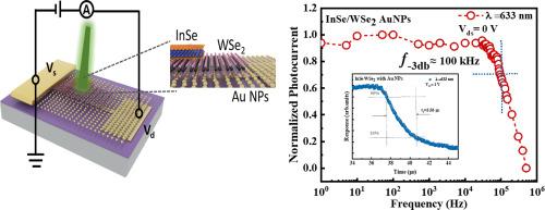
光电探测器在军事防御、航空航天和成像领域至关重要。二维过渡金属二硫族化合物(TMDs)因其可调的带隙和强的光-物质相互作用而备受关注,但其有限的厚度限制了其光吸收。在本研究中,通过金纳米粒子(Au NPs)修饰结构和铟膜表面功能化,系统地探索了表面等离子体共振和表面工程对材料InSe/WSe2异质结构光电性能的影响。通过将Au NPs与InSe/WSe2异质结集成并使用铟层功能化异质结表面,该器件在400至1550 nm的宽带光谱范围内表现出显著的光吸收增强。与原始的InSe/WSe2异质结相比,该器件在室温和零偏置电压下工作,显示出相当大的光电性能改善。具体而言,该器件的响应率为1.39 a /W,探测率为4.23 × 1011 Jones,响应时间为2.7 μs。这些卓越的性能特征,结合金属纳米结构的可扩展和可控制造的优势,以及二维材料合成和转移技术的进步,展示了大规模、智能制造低功耗、纳米级光电器件的巨大潜力。
Ultrafast Self-Powered photodetector based on Plasmon-assisted InSe/WSe2 van der Waals heterostructures
Photodetectors are vital in military defense, aerospace, and imaging. Two-dimensional transition metal dichalcogenides (TMDs) attract attention for their tunable bandgap and strong light-matter interaction, but their limited thickness restricts light absorption. In this study, the influence of surface plasmon resonance and surface engineering on the InSe/WSe2 heterostructures optoelectronic properties of the material was systematically explored by modifying the structure with gold nanoparticles (Au NPs) and functionalizing the indium film surface. By integrating Au NPs with the InSe/WSe2 heterojunction and functionalizing the heterojunction surface using an indium layer, the device exhibited a significant enhancement in light absorption over a broadband spectral range from 447 to 1550 nm. Operating at room temperature and under zero bias voltage, the device showed a considerable improvement in optoelectronic performance compared to the pristine InSe/WSe2 heterojunction. Specifically, the device achieved a responsivity of 1.39 A/W, a detectivity of 4.23 × 10¹¹ Jones, and an ultra-fast response time of 2.7 μs. These remarkable performance characteristics, combined with the advantages of scalable and controlled fabrication of metallic nanostructures, along with advancements in 2D material synthesis and transfer techniques, demonstrate significant potential for the large-scale, smart manufacturing of low-power, nanoscale optoelectronic devices.
期刊介绍:
Applied Surface Science covers topics contributing to a better understanding of surfaces, interfaces, nanostructures and their applications. The journal is concerned with scientific research on the atomic and molecular level of material properties determined with specific surface analytical techniques and/or computational methods, as well as the processing of such structures.