用于高电流密度有机纳米线晶体管和栅极可调光发射的可转移聚合物绝缘纳米网电极

IF 6.7 1区 物理与天体物理 Q1 MATERIALS SCIENCE, MULTIDISCIPLINARY
Baichuan Jiang, Zhagen Miao, Yingxuan Zhao, Can Gao, Wenbin Li, Huanli Dong, Cailing Ou, Jun Li, Nannan Dou, Tingyu Ji, Zixiao Han, Xiaoru Cao, Paolo Samorì, Lei Zhang
{"title":"用于高电流密度有机纳米线晶体管和栅极可调光发射的可转移聚合物绝缘纳米网电极","authors":"Baichuan Jiang, Zhagen Miao, Yingxuan Zhao, Can Gao, Wenbin Li, Huanli Dong, Cailing Ou, Jun Li, Nannan Dou, Tingyu Ji, Zixiao Han, Xiaoru Cao, Paolo Samorì, Lei Zhang","doi":"10.1021/acsphotonics.5c00576","DOIUrl":null,"url":null,"abstract":"Harnessing the full potential of a gate-modulated planar junction to maximize its on-state current density presents fundamental challenges in nanotechnology, particularly for semiconducting nanowires due to their random orientations and partial coverage. Herein, we developed a straightforward method by combining dual self-alignment with nanosphere lithography to fabricate a nanomesh electrode conformally encapsulated by a polymeric insulator. This honeycomb-like nanostructured electrode is designed to form a vertically stacked electrode pair with the (semi)conducting materials precisely filling its pores. For a 200 μm × 200 μm transistor area, the channel width-to-length ratio is expected to approach 7.6 × 10<sup>5</sup>, effectively achieving a patterning resolution of 100–200 nm without requiring expensive nanofabrication tools such as photolithography and electron-beam lithography. The resulting field-effect transistors using supramolecular poly(3-hexylthiophene) nanowires as the channel active layer exhibited a maximum on-state current density exceeding 2000 mA cm<sup>–2</sup>. Additionally, the integration of a light-emitting junction by vacuum-depositing tris(8-hydroxyquinolinato) aluminum atop results in gate-modulated uniform luminance up to 1000 cd m<sup>–2</sup>. This approach paves the way for highly integrated applications, such as micro-LED pixel driving, by maximizing the transistor current density based on a given metal–insulator-semiconductor junction.","PeriodicalId":23,"journal":{"name":"ACS Photonics","volume":"16 1","pages":""},"PeriodicalIF":6.7000,"publicationDate":"2025-05-29","publicationTypes":"Journal Article","fieldsOfStudy":null,"isOpenAccess":false,"openAccessPdf":"","citationCount":"0","resultStr":"{\"title\":\"Transferable, Polymer-Insulated Nanomesh Electrode for High-Current-Density Organic Nanowire Transistors and Gate-Tunable Light Emission\",\"authors\":\"Baichuan Jiang, Zhagen Miao, Yingxuan Zhao, Can Gao, Wenbin Li, Huanli Dong, Cailing Ou, Jun Li, Nannan Dou, Tingyu Ji, Zixiao Han, Xiaoru Cao, Paolo Samorì, Lei Zhang\",\"doi\":\"10.1021/acsphotonics.5c00576\",\"DOIUrl\":null,\"url\":null,\"abstract\":\"Harnessing the full potential of a gate-modulated planar junction to maximize its on-state current density presents fundamental challenges in nanotechnology, particularly for semiconducting nanowires due to their random orientations and partial coverage. Herein, we developed a straightforward method by combining dual self-alignment with nanosphere lithography to fabricate a nanomesh electrode conformally encapsulated by a polymeric insulator. This honeycomb-like nanostructured electrode is designed to form a vertically stacked electrode pair with the (semi)conducting materials precisely filling its pores. For a 200 μm × 200 μm transistor area, the channel width-to-length ratio is expected to approach 7.6 × 10<sup>5</sup>, effectively achieving a patterning resolution of 100–200 nm without requiring expensive nanofabrication tools such as photolithography and electron-beam lithography. The resulting field-effect transistors using supramolecular poly(3-hexylthiophene) nanowires as the channel active layer exhibited a maximum on-state current density exceeding 2000 mA cm<sup>–2</sup>. Additionally, the integration of a light-emitting junction by vacuum-depositing tris(8-hydroxyquinolinato) aluminum atop results in gate-modulated uniform luminance up to 1000 cd m<sup>–2</sup>. This approach paves the way for highly integrated applications, such as micro-LED pixel driving, by maximizing the transistor current density based on a given metal–insulator-semiconductor junction.\",\"PeriodicalId\":23,\"journal\":{\"name\":\"ACS Photonics\",\"volume\":\"16 1\",\"pages\":\"\"},\"PeriodicalIF\":6.7000,\"publicationDate\":\"2025-05-29\",\"publicationTypes\":\"Journal Article\",\"fieldsOfStudy\":null,\"isOpenAccess\":false,\"openAccessPdf\":\"\",\"citationCount\":\"0\",\"resultStr\":null,\"platform\":\"Semanticscholar\",\"paperid\":null,\"PeriodicalName\":\"ACS Photonics\",\"FirstCategoryId\":\"101\",\"ListUrlMain\":\"https://doi.org/10.1021/acsphotonics.5c00576\",\"RegionNum\":1,\"RegionCategory\":\"物理与天体物理\",\"ArticlePicture\":[],\"TitleCN\":null,\"AbstractTextCN\":null,\"PMCID\":null,\"EPubDate\":\"\",\"PubModel\":\"\",\"JCR\":\"Q1\",\"JCRName\":\"MATERIALS SCIENCE, MULTIDISCIPLINARY\",\"Score\":null,\"Total\":0}","platform":"Semanticscholar","paperid":null,"PeriodicalName":"ACS Photonics","FirstCategoryId":"101","ListUrlMain":"https://doi.org/10.1021/acsphotonics.5c00576","RegionNum":1,"RegionCategory":"物理与天体物理","ArticlePicture":[],"TitleCN":null,"AbstractTextCN":null,"PMCID":null,"EPubDate":"","PubModel":"","JCR":"Q1","JCRName":"MATERIALS SCIENCE, MULTIDISCIPLINARY","Score":null,"Total":0}
引用次数: 0

摘要

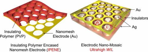
利用栅极调制平面结的全部潜力来最大化其导通电流密度是纳米技术的基本挑战,特别是半导体纳米线由于其随机方向和部分覆盖而面临的挑战。在此,我们开发了一种简单的方法,将双自对准与纳米球光刻相结合,制造出由聚合物绝缘体共形封装的纳米网格电极。这种蜂窝状的纳米结构电极被设计成垂直堆叠的电极对,(半)导电材料精确地填充其孔隙。对于200 μm × 200 μm的晶体管面积,通道宽度与长度比预计将接近7.6 × 10⁵,有效地实现100-200 nm的图案分辨率,而不需要昂贵的纳米制造工具,如光刻和电子束光刻。采用超分子聚(3-己基噻吩)纳米线作为沟道有源层的场效应晶体管的最大导通电流密度超过2000 mA cm-2。此外,通过真空沉积三(8-羟基喹啉)铝顶部的发光结集成导致门调制均匀亮度高达1000 cd - m-2。这种方法通过最大化基于给定金属-绝缘体-半导体结的晶体管电流密度,为高度集成的应用铺平了道路,例如微型led像素驱动。
本文章由计算机程序翻译,如有差异,请以英文原文为准。

Transferable, Polymer-Insulated Nanomesh Electrode for High-Current-Density Organic Nanowire Transistors and Gate-Tunable Light Emission

Transferable, Polymer-Insulated Nanomesh Electrode for High-Current-Density Organic Nanowire Transistors and Gate-Tunable Light Emission
Harnessing the full potential of a gate-modulated planar junction to maximize its on-state current density presents fundamental challenges in nanotechnology, particularly for semiconducting nanowires due to their random orientations and partial coverage. Herein, we developed a straightforward method by combining dual self-alignment with nanosphere lithography to fabricate a nanomesh electrode conformally encapsulated by a polymeric insulator. This honeycomb-like nanostructured electrode is designed to form a vertically stacked electrode pair with the (semi)conducting materials precisely filling its pores. For a 200 μm × 200 μm transistor area, the channel width-to-length ratio is expected to approach 7.6 × 10⁵, effectively achieving a patterning resolution of 100–200 nm without requiring expensive nanofabrication tools such as photolithography and electron-beam lithography. The resulting field-effect transistors using supramolecular poly(3-hexylthiophene) nanowires as the channel active layer exhibited a maximum on-state current density exceeding 2000 mA cm–2. Additionally, the integration of a light-emitting junction by vacuum-depositing tris(8-hydroxyquinolinato) aluminum atop results in gate-modulated uniform luminance up to 1000 cd m–2. This approach paves the way for highly integrated applications, such as micro-LED pixel driving, by maximizing the transistor current density based on a given metal–insulator-semiconductor junction.
求助全文
通过发布文献求助,成功后即可免费获取论文全文。 去求助
来源期刊
ACS Photonics
ACS Photonics NANOSCIENCE & NANOTECHNOLOGY-MATERIALS SCIENCE, MULTIDISCIPLINARY
CiteScore
11.90
自引率
5.70%
发文量
438
审稿时长
2.3 months
期刊介绍: Published as soon as accepted and summarized in monthly issues, ACS Photonics will publish Research Articles, Letters, Perspectives, and Reviews, to encompass the full scope of published research in this field.
×
引用
GB/T 7714-2015
复制
MLA
复制
APA
复制
导出至
BibTeX EndNote RefMan NoteFirst NoteExpress
×
提示
您的信息不完整,为了账户安全,请先补充。
现在去补充
×
提示
您因"违规操作"
具体请查看互助需知
我知道了
×
提示
确定
请完成安全验证×
copy
已复制链接
快去分享给好友吧!
我知道了
右上角分享
点击右上角分享
0
联系我们:info@booksci.cn Book学术提供免费学术资源搜索服务,方便国内外学者检索中英文文献。致力于提供最便捷和优质的服务体验。 Copyright © 2023 布克学术 All rights reserved.
京ICP备2023020795号-1
ghs 京公网安备 11010802042870号
Book学术文献互助
Book学术文献互助群
群 号:604180095
Book学术官方微信