原位CVD生长具有合金界面的WS2-MoS2横向异质结构:强光致发光增强和高开关比场效应晶体管

IF 8.2 2区 材料科学 Q1 MATERIALS SCIENCE, MULTIDISCIPLINARY
Abdul Kaium Mia , Sourav Dey , Lubomir Vanco , Viliam Vretenar , P.K. Giri
{"title":"原位CVD生长具有合金界面的WS2-MoS2横向异质结构:强光致发光增强和高开关比场效应晶体管","authors":"Abdul Kaium Mia ,&nbsp;Sourav Dey ,&nbsp;Lubomir Vanco ,&nbsp;Viliam Vretenar ,&nbsp;P.K. Giri","doi":"10.1016/j.mtnano.2025.100638","DOIUrl":null,"url":null,"abstract":"<div><div>The semiconducting 2D transition metal dichalcogenides (TMDs) have gained substantial attention, though the progress in their lateral heterostructures (HS) and in-situ growth for electronic and optoelectronic applications has been very limited. Herein, we report a single-step in-situ chemical vapor deposition growth of bilayer WS<sub>2</sub>-MoS<sub>2</sub> lateral HS, which ensures a clean diffused interface between WS<sub>2</sub> and MoS<sub>2,</sub> enabling efficient charge transport. The spatial Raman, photoluminescent (PL), and Auger mapping of in-situ WS<sub>2</sub>-MoS<sub>2</sub> lateral HS shows a clear transition from pure WS<sub>2</sub> to pure MoS<sub>2</sub> region through a graded WS<sub>(1-x)</sub>Mo<sub>x</sub>S<sub>2</sub> alloy interface. The composition and the width of the alloy interface could be tuned by careful choice of the proportion of precursor materials and by tuning the growth parameters. Spatially resolved PL spectra and PL mapping reveal a strongly enhanced (more than one order of magnitude) PL intensity in the HS interface attributed to the strain-induced bandstructure modification in the alloyed interface. Interestingly, the alloyed interface in the lateral HS also dramatically improves the electronic properties, resulting in an on-off ratio of 10<sup>8</sup> in the fabricated field effect transistor, which is two orders of magnitude higher than their individual counterpart. These results on lateral HS are significant, and they pave the way to synthesize other different HSs for future electronic devices and integrated circuits.</div></div>","PeriodicalId":48517,"journal":{"name":"Materials Today Nano","volume":"31 ","pages":"Article 100638"},"PeriodicalIF":8.2000,"publicationDate":"2025-05-22","publicationTypes":"Journal Article","fieldsOfStudy":null,"isOpenAccess":false,"openAccessPdf":"","citationCount":"0","resultStr":"{\"title\":\"In-situ CVD grown WS2-MoS2 lateral heterostructure with alloyed Interface: Strong photoluminescence enhancement and high on-off ratio field effect transistors\",\"authors\":\"Abdul Kaium Mia ,&nbsp;Sourav Dey ,&nbsp;Lubomir Vanco ,&nbsp;Viliam Vretenar ,&nbsp;P.K. Giri\",\"doi\":\"10.1016/j.mtnano.2025.100638\",\"DOIUrl\":null,\"url\":null,\"abstract\":\"<div><div>The semiconducting 2D transition metal dichalcogenides (TMDs) have gained substantial attention, though the progress in their lateral heterostructures (HS) and in-situ growth for electronic and optoelectronic applications has been very limited. Herein, we report a single-step in-situ chemical vapor deposition growth of bilayer WS<sub>2</sub>-MoS<sub>2</sub> lateral HS, which ensures a clean diffused interface between WS<sub>2</sub> and MoS<sub>2,</sub> enabling efficient charge transport. The spatial Raman, photoluminescent (PL), and Auger mapping of in-situ WS<sub>2</sub>-MoS<sub>2</sub> lateral HS shows a clear transition from pure WS<sub>2</sub> to pure MoS<sub>2</sub> region through a graded WS<sub>(1-x)</sub>Mo<sub>x</sub>S<sub>2</sub> alloy interface. The composition and the width of the alloy interface could be tuned by careful choice of the proportion of precursor materials and by tuning the growth parameters. Spatially resolved PL spectra and PL mapping reveal a strongly enhanced (more than one order of magnitude) PL intensity in the HS interface attributed to the strain-induced bandstructure modification in the alloyed interface. Interestingly, the alloyed interface in the lateral HS also dramatically improves the electronic properties, resulting in an on-off ratio of 10<sup>8</sup> in the fabricated field effect transistor, which is two orders of magnitude higher than their individual counterpart. These results on lateral HS are significant, and they pave the way to synthesize other different HSs for future electronic devices and integrated circuits.</div></div>\",\"PeriodicalId\":48517,\"journal\":{\"name\":\"Materials Today Nano\",\"volume\":\"31 \",\"pages\":\"Article 100638\"},\"PeriodicalIF\":8.2000,\"publicationDate\":\"2025-05-22\",\"publicationTypes\":\"Journal Article\",\"fieldsOfStudy\":null,\"isOpenAccess\":false,\"openAccessPdf\":\"\",\"citationCount\":\"0\",\"resultStr\":null,\"platform\":\"Semanticscholar\",\"paperid\":null,\"PeriodicalName\":\"Materials Today Nano\",\"FirstCategoryId\":\"88\",\"ListUrlMain\":\"https://www.sciencedirect.com/science/article/pii/S2588842025000690\",\"RegionNum\":2,\"RegionCategory\":\"材料科学\",\"ArticlePicture\":[],\"TitleCN\":null,\"AbstractTextCN\":null,\"PMCID\":null,\"EPubDate\":\"\",\"PubModel\":\"\",\"JCR\":\"Q1\",\"JCRName\":\"MATERIALS SCIENCE, MULTIDISCIPLINARY\",\"Score\":null,\"Total\":0}","platform":"Semanticscholar","paperid":null,"PeriodicalName":"Materials Today Nano","FirstCategoryId":"88","ListUrlMain":"https://www.sciencedirect.com/science/article/pii/S2588842025000690","RegionNum":2,"RegionCategory":"材料科学","ArticlePicture":[],"TitleCN":null,"AbstractTextCN":null,"PMCID":null,"EPubDate":"","PubModel":"","JCR":"Q1","JCRName":"MATERIALS SCIENCE, MULTIDISCIPLINARY","Score":null,"Total":0}
引用次数: 0

摘要

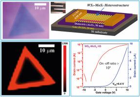
半导体二维过渡金属二硫族化合物(TMDs)已经引起了广泛的关注,尽管其横向异质结构(HS)和原位生长在电子和光电应用方面的进展非常有限。在此,我们报道了一种单步原位化学气相沉积生长WS2-MoS2双层横向HS,它确保了WS2和MoS2之间清洁的扩散界面,实现了高效的电荷传输。原位WS2-MoS2横向HS的空间拉曼、光致发光(PL)和俄格图显示,通过渐变的WS(1-x)MoxS2合金界面,从纯WS2区明显过渡到纯MoS2区。通过仔细选择前驱体材料的比例和调整生长参数,可以调整合金界面的组成和宽度。空间分辨PL光谱和PL映射显示,由于合金界面中应变诱导的带结构改变,HS界面中的PL强度明显增强(超过一个数量级)。有趣的是,横向HS中的合金界面也显著提高了电子性能,导致制造的场效应晶体管的通断比为108,比单独的场效应晶体管高出两个数量级。这些横向HS的研究结果具有重要意义,为未来电子器件和集成电路合成其他不同HS铺平了道路。
本文章由计算机程序翻译,如有差异,请以英文原文为准。

In-situ CVD grown WS2-MoS2 lateral heterostructure with alloyed Interface: Strong photoluminescence enhancement and high on-off ratio field effect transistors

In-situ CVD grown WS2-MoS2 lateral heterostructure with alloyed Interface: Strong photoluminescence enhancement and high on-off ratio field effect transistors
The semiconducting 2D transition metal dichalcogenides (TMDs) have gained substantial attention, though the progress in their lateral heterostructures (HS) and in-situ growth for electronic and optoelectronic applications has been very limited. Herein, we report a single-step in-situ chemical vapor deposition growth of bilayer WS2-MoS2 lateral HS, which ensures a clean diffused interface between WS2 and MoS2, enabling efficient charge transport. The spatial Raman, photoluminescent (PL), and Auger mapping of in-situ WS2-MoS2 lateral HS shows a clear transition from pure WS2 to pure MoS2 region through a graded WS(1-x)MoxS2 alloy interface. The composition and the width of the alloy interface could be tuned by careful choice of the proportion of precursor materials and by tuning the growth parameters. Spatially resolved PL spectra and PL mapping reveal a strongly enhanced (more than one order of magnitude) PL intensity in the HS interface attributed to the strain-induced bandstructure modification in the alloyed interface. Interestingly, the alloyed interface in the lateral HS also dramatically improves the electronic properties, resulting in an on-off ratio of 108 in the fabricated field effect transistor, which is two orders of magnitude higher than their individual counterpart. These results on lateral HS are significant, and they pave the way to synthesize other different HSs for future electronic devices and integrated circuits.
求助全文
通过发布文献求助,成功后即可免费获取论文全文。 去求助
来源期刊
CiteScore
11.30
自引率
3.90%
发文量
130
审稿时长
31 days
期刊介绍: Materials Today Nano is a multidisciplinary journal dedicated to nanoscience and nanotechnology. The journal aims to showcase the latest advances in nanoscience and provide a platform for discussing new concepts and applications. With rigorous peer review, rapid decisions, and high visibility, Materials Today Nano offers authors the opportunity to publish comprehensive articles, short communications, and reviews on a wide range of topics in nanoscience. The editors welcome comprehensive articles, short communications and reviews on topics including but not limited to: Nanoscale synthesis and assembly Nanoscale characterization Nanoscale fabrication Nanoelectronics and molecular electronics Nanomedicine Nanomechanics Nanosensors Nanophotonics Nanocomposites
×
引用
GB/T 7714-2015
复制
MLA
复制
APA
复制
导出至
BibTeX EndNote RefMan NoteFirst NoteExpress
×
提示
您的信息不完整,为了账户安全,请先补充。
现在去补充
×
提示
您因"违规操作"
具体请查看互助需知
我知道了
×
提示
确定
请完成安全验证×
copy
已复制链接
快去分享给好友吧!
我知道了
右上角分享
点击右上角分享
0
联系我们:info@booksci.cn Book学术提供免费学术资源搜索服务,方便国内外学者检索中英文文献。致力于提供最便捷和优质的服务体验。 Copyright © 2023 布克学术 All rights reserved.
京ICP备2023020795号-1
ghs 京公网安备 11010802042870号
Book学术文献互助
Book学术文献互助群
群 号:604180095
Book学术官方微信