Bich Phuong Nguyen, Sarah Su-O Youn, Yeon Soo Kim, Thuy Thi Nguyen, Ha Kyung Park, Gee Yeong Kim and William Jo
{"title":"稳定光电器件中2D-3D钙钛矿混合物的自由载流子输运和离子迁移","authors":"Bich Phuong Nguyen, Sarah Su-O Youn, Yeon Soo Kim, Thuy Thi Nguyen, Ha Kyung Park, Gee Yeong Kim and William Jo","doi":"10.1039/D5NR00992H","DOIUrl":null,"url":null,"abstract":"<p >Manipulating charge carrier recombination dynamics in mixed three-dimensional (3D) and two-dimensional (2D) perovskites is an effective approach to enhance performance and long-term stability in both solar cells and light-emitting diodes (LEDs). Due to high crystallinity and a low charge carrier recombination coefficient, photogenerated charge carriers in solar cells can effectively diffuse across the perovskite layer, while enhancing radiative recombination through charge carrier confinement can significantly improve electroluminescence efficiencies in LEDs. Further improvements in device efficiency and stability require a comprehensive understanding of charge carrier transport at the numerous interfaces between the different phases of 2D perovskites at both the micro- and nanoscale, as well as ion migration. In this study, we examine the carrier transport mechanism at the thin-surface 2D/bulk 3D perovskite interface and the dense-surface 2D/3D heterophase. The electrical properties and ion migration behavior were analyzed by examining the transition of the <em>J</em>–<em>V</em> characteristics in both vertical and lateral devices. We carefully analyzed the influence of nanostructures on charge transport using conductive atomic force microscopy (C-AFM) and Kelvin probe force microscopy (KPFM). The variation in the spatial response of the photocurrent and surface photovoltage across grains and grain boundaries with different phases of the 2D perovskite was carefully examined. These insights provide a pathway for optimizing the electrical properties and charge transport behavior of mixed perovskites, further positioning them as key materials for the development of efficient and stable optoelectronic devices.</p>","PeriodicalId":92,"journal":{"name":"Nanoscale","volume":" 25","pages":" 15239-15251"},"PeriodicalIF":5.1000,"publicationDate":"2025-05-28","publicationTypes":"Journal Article","fieldsOfStudy":null,"isOpenAccess":false,"openAccessPdf":"https://pubs.rsc.org/en/content/articlepdf/2025/nr/d5nr00992h?page=search","citationCount":"0","resultStr":"{\"title\":\"Unveiling of free carrier transport and ion migration in a 2D–3D perovskite mixture for stable optoelectronic devices†\",\"authors\":\"Bich Phuong Nguyen, Sarah Su-O Youn, Yeon Soo Kim, Thuy Thi Nguyen, Ha Kyung Park, Gee Yeong Kim and William Jo\",\"doi\":\"10.1039/D5NR00992H\",\"DOIUrl\":null,\"url\":null,\"abstract\":\"<p >Manipulating charge carrier recombination dynamics in mixed three-dimensional (3D) and two-dimensional (2D) perovskites is an effective approach to enhance performance and long-term stability in both solar cells and light-emitting diodes (LEDs). Due to high crystallinity and a low charge carrier recombination coefficient, photogenerated charge carriers in solar cells can effectively diffuse across the perovskite layer, while enhancing radiative recombination through charge carrier confinement can significantly improve electroluminescence efficiencies in LEDs. Further improvements in device efficiency and stability require a comprehensive understanding of charge carrier transport at the numerous interfaces between the different phases of 2D perovskites at both the micro- and nanoscale, as well as ion migration. In this study, we examine the carrier transport mechanism at the thin-surface 2D/bulk 3D perovskite interface and the dense-surface 2D/3D heterophase. The electrical properties and ion migration behavior were analyzed by examining the transition of the <em>J</em>–<em>V</em> characteristics in both vertical and lateral devices. We carefully analyzed the influence of nanostructures on charge transport using conductive atomic force microscopy (C-AFM) and Kelvin probe force microscopy (KPFM). The variation in the spatial response of the photocurrent and surface photovoltage across grains and grain boundaries with different phases of the 2D perovskite was carefully examined. These insights provide a pathway for optimizing the electrical properties and charge transport behavior of mixed perovskites, further positioning them as key materials for the development of efficient and stable optoelectronic devices.</p>\",\"PeriodicalId\":92,\"journal\":{\"name\":\"Nanoscale\",\"volume\":\" 25\",\"pages\":\" 15239-15251\"},\"PeriodicalIF\":5.1000,\"publicationDate\":\"2025-05-28\",\"publicationTypes\":\"Journal Article\",\"fieldsOfStudy\":null,\"isOpenAccess\":false,\"openAccessPdf\":\"https://pubs.rsc.org/en/content/articlepdf/2025/nr/d5nr00992h?page=search\",\"citationCount\":\"0\",\"resultStr\":null,\"platform\":\"Semanticscholar\",\"paperid\":null,\"PeriodicalName\":\"Nanoscale\",\"FirstCategoryId\":\"88\",\"ListUrlMain\":\"https://pubs.rsc.org/en/content/articlelanding/2025/nr/d5nr00992h\",\"RegionNum\":3,\"RegionCategory\":\"材料科学\",\"ArticlePicture\":[],\"TitleCN\":null,\"AbstractTextCN\":null,\"PMCID\":null,\"EPubDate\":\"\",\"PubModel\":\"\",\"JCR\":\"Q1\",\"JCRName\":\"CHEMISTRY, MULTIDISCIPLINARY\",\"Score\":null,\"Total\":0}","platform":"Semanticscholar","paperid":null,"PeriodicalName":"Nanoscale","FirstCategoryId":"88","ListUrlMain":"https://pubs.rsc.org/en/content/articlelanding/2025/nr/d5nr00992h","RegionNum":3,"RegionCategory":"材料科学","ArticlePicture":[],"TitleCN":null,"AbstractTextCN":null,"PMCID":null,"EPubDate":"","PubModel":"","JCR":"Q1","JCRName":"CHEMISTRY, MULTIDISCIPLINARY","Score":null,"Total":0}
Unveiling of free carrier transport and ion migration in a 2D–3D perovskite mixture for stable optoelectronic devices†
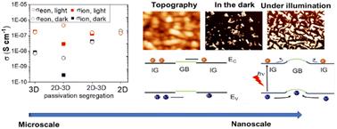
Manipulating charge carrier recombination dynamics in mixed three-dimensional (3D) and two-dimensional (2D) perovskites is an effective approach to enhance performance and long-term stability in both solar cells and light-emitting diodes (LEDs). Due to high crystallinity and a low charge carrier recombination coefficient, photogenerated charge carriers in solar cells can effectively diffuse across the perovskite layer, while enhancing radiative recombination through charge carrier confinement can significantly improve electroluminescence efficiencies in LEDs. Further improvements in device efficiency and stability require a comprehensive understanding of charge carrier transport at the numerous interfaces between the different phases of 2D perovskites at both the micro- and nanoscale, as well as ion migration. In this study, we examine the carrier transport mechanism at the thin-surface 2D/bulk 3D perovskite interface and the dense-surface 2D/3D heterophase. The electrical properties and ion migration behavior were analyzed by examining the transition of the J–V characteristics in both vertical and lateral devices. We carefully analyzed the influence of nanostructures on charge transport using conductive atomic force microscopy (C-AFM) and Kelvin probe force microscopy (KPFM). The variation in the spatial response of the photocurrent and surface photovoltage across grains and grain boundaries with different phases of the 2D perovskite was carefully examined. These insights provide a pathway for optimizing the electrical properties and charge transport behavior of mixed perovskites, further positioning them as key materials for the development of efficient and stable optoelectronic devices.
期刊介绍:
Nanoscale is a high-impact international journal, publishing high-quality research across nanoscience and nanotechnology. Nanoscale publishes a full mix of research articles on experimental and theoretical work, including reviews, communications, and full papers.Highly interdisciplinary, this journal appeals to scientists, researchers and professionals interested in nanoscience and nanotechnology, quantum materials and quantum technology, including the areas of physics, chemistry, biology, medicine, materials, energy/environment, information technology, detection science, healthcare and drug discovery, and electronics.

 求助内容:
求助内容: 应助结果提醒方式:


