{"title":"基于隧道异质结构MoS2/PdSe2的高性能宽带光电探测器","authors":"Weijing Liu, Xiaozhendong Bao, Yifan Zhou, Junyun Meng, Siyuan Qi, Yuee Xie, Yuanping Chen","doi":"10.1021/acsami.5c00847","DOIUrl":null,"url":null,"abstract":"The two-dimensional (2D) material PdSe<sub>2</sub> is an ideal material for preparing a high-performance broadband photodetector because of its narrow and tunable band gap. However, poor light absorption limits the application of single PdSe<sub>2</sub>. Here, a PdSe<sub>2</sub>-based van der Waals (vdWs) heterostructure MoS<sub>2</sub>/PdSe<sub>2</sub> is selected to realize broadband photodetection after a screening of theoretical calculations. Different from most other PdSe<sub>2</sub>-based heterostructures, MoS<sub>2</sub>/PdSe<sub>2</sub> here is a heterostructure with a type-I band alignment, where the conduction band minimum (CBM) and valence band maximum (VBM) both come from PdSe<sub>2</sub>. It exhibits high-performance broadband photodetection, for example, in the case of a 600 nm illumination, the heterostructure shows a responsivity of 51.4 A/W and a detectivity of 2.28 × 10<sup>10</sup> cm Hz<sup>1/2</sup> W<sup>–1</sup>; in the case of a near-infrared illumination of 900 nm, it has a responsivity of 6.11 A/W and a detectivity of 2.71 × 10<sup>9</sup> cm Hz<sup>1/2</sup> W<sup>–1</sup>. Our analysis indicates that the good performance originates from a direct tunneling (DT) mechanism in the heterostructure, which not only reduces the recombination of carriers but also improves the carrier collection rate.","PeriodicalId":5,"journal":{"name":"ACS Applied Materials & Interfaces","volume":"19 1","pages":""},"PeriodicalIF":8.2000,"publicationDate":"2025-05-21","publicationTypes":"Journal Article","fieldsOfStudy":null,"isOpenAccess":false,"openAccessPdf":"","citationCount":"0","resultStr":"{\"title\":\"High-Performance Broadband Photodetector Based on Tunneling Heterostructure MoS2/PdSe2\",\"authors\":\"Weijing Liu, Xiaozhendong Bao, Yifan Zhou, Junyun Meng, Siyuan Qi, Yuee Xie, Yuanping Chen\",\"doi\":\"10.1021/acsami.5c00847\",\"DOIUrl\":null,\"url\":null,\"abstract\":\"The two-dimensional (2D) material PdSe<sub>2</sub> is an ideal material for preparing a high-performance broadband photodetector because of its narrow and tunable band gap. However, poor light absorption limits the application of single PdSe<sub>2</sub>. Here, a PdSe<sub>2</sub>-based van der Waals (vdWs) heterostructure MoS<sub>2</sub>/PdSe<sub>2</sub> is selected to realize broadband photodetection after a screening of theoretical calculations. Different from most other PdSe<sub>2</sub>-based heterostructures, MoS<sub>2</sub>/PdSe<sub>2</sub> here is a heterostructure with a type-I band alignment, where the conduction band minimum (CBM) and valence band maximum (VBM) both come from PdSe<sub>2</sub>. It exhibits high-performance broadband photodetection, for example, in the case of a 600 nm illumination, the heterostructure shows a responsivity of 51.4 A/W and a detectivity of 2.28 × 10<sup>10</sup> cm Hz<sup>1/2</sup> W<sup>–1</sup>; in the case of a near-infrared illumination of 900 nm, it has a responsivity of 6.11 A/W and a detectivity of 2.71 × 10<sup>9</sup> cm Hz<sup>1/2</sup> W<sup>–1</sup>. Our analysis indicates that the good performance originates from a direct tunneling (DT) mechanism in the heterostructure, which not only reduces the recombination of carriers but also improves the carrier collection rate.\",\"PeriodicalId\":5,\"journal\":{\"name\":\"ACS Applied Materials & Interfaces\",\"volume\":\"19 1\",\"pages\":\"\"},\"PeriodicalIF\":8.2000,\"publicationDate\":\"2025-05-21\",\"publicationTypes\":\"Journal Article\",\"fieldsOfStudy\":null,\"isOpenAccess\":false,\"openAccessPdf\":\"\",\"citationCount\":\"0\",\"resultStr\":null,\"platform\":\"Semanticscholar\",\"paperid\":null,\"PeriodicalName\":\"ACS Applied Materials & Interfaces\",\"FirstCategoryId\":\"88\",\"ListUrlMain\":\"https://doi.org/10.1021/acsami.5c00847\",\"RegionNum\":2,\"RegionCategory\":\"材料科学\",\"ArticlePicture\":[],\"TitleCN\":null,\"AbstractTextCN\":null,\"PMCID\":null,\"EPubDate\":\"\",\"PubModel\":\"\",\"JCR\":\"Q1\",\"JCRName\":\"MATERIALS SCIENCE, MULTIDISCIPLINARY\",\"Score\":null,\"Total\":0}","platform":"Semanticscholar","paperid":null,"PeriodicalName":"ACS Applied Materials & Interfaces","FirstCategoryId":"88","ListUrlMain":"https://doi.org/10.1021/acsami.5c00847","RegionNum":2,"RegionCategory":"材料科学","ArticlePicture":[],"TitleCN":null,"AbstractTextCN":null,"PMCID":null,"EPubDate":"","PubModel":"","JCR":"Q1","JCRName":"MATERIALS SCIENCE, MULTIDISCIPLINARY","Score":null,"Total":0}
引用次数: 0
摘要
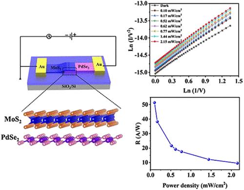
二维(2D)材料PdSe2是制备高性能宽带光电探测器的理想材料,因为其窄且可调谐的带隙。然而,较差的光吸收限制了单个PdSe2的应用。本文在理论计算筛选后,选择基于PdSe2的范德华(vdWs)异质结构MoS2/PdSe2实现宽带光探测。与其他大多数基于PdSe2的异质结构不同,MoS2/PdSe2是一种具有i型带取向的异质结构,其中导带最小值(CBM)和价带最大值(VBM)都来自PdSe2。在600 nm光照条件下,该异质结构的响应度为51.4 a /W,探测率为2.28 × 1010 cm Hz1/2 W - 1;在900 nm的近红外光照下,其响应度为6.11 a /W,探测率为2.71 × 109 cm Hz1/2 W - 1。我们的分析表明,良好的性能源于异质结构中的直接隧道(DT)机制,这不仅减少了载流子的重组,而且提高了载流子的收集率。
High-Performance Broadband Photodetector Based on Tunneling Heterostructure MoS2/PdSe2
The two-dimensional (2D) material PdSe2 is an ideal material for preparing a high-performance broadband photodetector because of its narrow and tunable band gap. However, poor light absorption limits the application of single PdSe2. Here, a PdSe2-based van der Waals (vdWs) heterostructure MoS2/PdSe2 is selected to realize broadband photodetection after a screening of theoretical calculations. Different from most other PdSe2-based heterostructures, MoS2/PdSe2 here is a heterostructure with a type-I band alignment, where the conduction band minimum (CBM) and valence band maximum (VBM) both come from PdSe2. It exhibits high-performance broadband photodetection, for example, in the case of a 600 nm illumination, the heterostructure shows a responsivity of 51.4 A/W and a detectivity of 2.28 × 1010 cm Hz1/2 W–1; in the case of a near-infrared illumination of 900 nm, it has a responsivity of 6.11 A/W and a detectivity of 2.71 × 109 cm Hz1/2 W–1. Our analysis indicates that the good performance originates from a direct tunneling (DT) mechanism in the heterostructure, which not only reduces the recombination of carriers but also improves the carrier collection rate.
期刊介绍:
ACS Applied Materials & Interfaces is a leading interdisciplinary journal that brings together chemists, engineers, physicists, and biologists to explore the development and utilization of newly-discovered materials and interfacial processes for specific applications. Our journal has experienced remarkable growth since its establishment in 2009, both in terms of the number of articles published and the impact of the research showcased. We are proud to foster a truly global community, with the majority of published articles originating from outside the United States, reflecting the rapid growth of applied research worldwide.