用于纳米分析物传感的介电泳增强石墨烯场效应晶体管
IF 8.2
2区 材料科学
Q1 MATERIALS SCIENCE, MULTIDISCIPLINARY
引用次数: 0
摘要
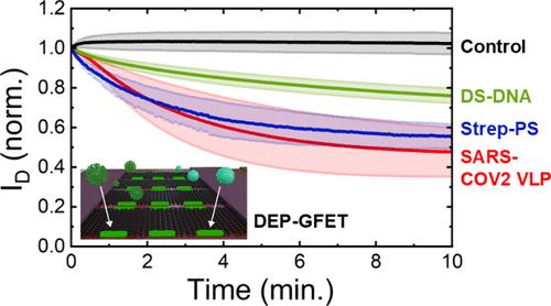
介电泳(DEP)传感是一种非常重要的传感方式,可以快速捕获和检测纳米级极化颗粒。这使得它成为医学诊断、环境监测和材料科学应用的通用工具。由于DEP依赖于产生尖锐的电极边缘,其灵敏度从根本上受到电极厚度的限制。石墨烯具有单层厚度,可以缩放DEP力,允许在超低电压下将颗粒捕获在石墨烯边缘。然而,到目前为止,这种增强的石墨烯捕获效率尚未转化为有效的传感几何结构。在这里,我们展示了石墨烯DEP捕获能力扩展到石墨烯场效应晶体管(GFET)的几何形状,使捕获的粒子能够被电检测。这种四端多功能混合器件结构有三种不同的工作模式:DEP、GFET和DEP-GFET。通过将GFET的通道分割成多个平行通道,荧光显微镜分析显示粒子捕获密度大大增加。我们展示了利用工程“纳米位点”进一步提高捕获效率,纳米位点是石墨烯中大小为200-300纳米的孔。对固定金纳米粒子(AuNPs)的扫描电镜分析表明,对于适当设计的纳米位点,捕获效率为90%。我们还演示了对AuNPs的实时、快速电传感,在4.1 s内发生>;2%的电流变化,以及对各种生物分子包被纳米颗粒的快速传感。这项工作表明,石墨烯DEP是纳米粒子和生物分子传感的有效平台,可以克服扩散限制和布朗运动相互作用。本文章由计算机程序翻译,如有差异,请以英文原文为准。
Dielectrophoresis-Enhanced Graphene Field-Effect Transistors for Nano-Analyte Sensing
Dielectrophoretic (DEP) sensing is an extremely important sensing modality that enables the rapid capture and detection of polarizable particles of nanoscale size. This makes it a versatile tool for applications in medical diagnostics, environmental monitoring, and materials science. Because DEP relies upon the creation of sharp electrode edges, its sensitivity is fundamentally limited by the electrode thickness. Graphene, with its monolayer thickness, enables scaling of the DEP force, allowing trapping of particles at graphene edges at ultralow voltages. However, to date, this enhanced trapping efficiency of graphene has not been translated into an effective sensing geometry. Here, we demonstrate the expansion of graphene DEP trapping capability into a graphene field effect transistor (GFET) geometry that allows the trapped particles to be electrically detected. This four-terminal multifunctional hybrid device structure operates in three distinct modes: DEP, GFET, and DEP-GFET. By segmenting the channel of the GFET into multiple parallel channels, greatly increased density of particle trapping is demonstrated using fluorescence microscopy analysis. We show further enhancement of the trapping efficiency using engineered “nanosites,” which are holes in the graphene with size on the order of 200–300 nm. Scanning electron microscope analysis of immobilized gold nanoparticles (AuNPs) shows trapping efficiency >90% for properly engineered nanosites. We also demonstrate real-time, rapid electrical sensing of AuNPs, with >2% current change occurring in 4.1 s, as well as rapid sensing of a variety of biomolecule-coated nanoparticles. This work shows that graphene DEP is an effective platform for nanoparticle and biomolecule sensing that overcomes diffusion-limited and Brownian motion-based interactions.
求助全文
通过发布文献求助,成功后即可免费获取论文全文。
去求助
来源期刊

ACS Applied Materials & Interfaces
工程技术-材料科学:综合
CiteScore
16.00
自引率
6.30%
发文量
4978
审稿时长
1.8 months
期刊介绍:
ACS Applied Materials & Interfaces is a leading interdisciplinary journal that brings together chemists, engineers, physicists, and biologists to explore the development and utilization of newly-discovered materials and interfacial processes for specific applications. Our journal has experienced remarkable growth since its establishment in 2009, both in terms of the number of articles published and the impact of the research showcased. We are proud to foster a truly global community, with the majority of published articles originating from outside the United States, reflecting the rapid growth of applied research worldwide.
 求助内容:
求助内容: 应助结果提醒方式:


