氮化镓纳米棒的p型表面缺陷

IF 9.1 1区 材料科学 Q1 CHEMISTRY, MULTIDISCIPLINARY
Sumesh Sadhujan, Sherina Harilal, Kefan Zhang, Riam Abu Much, Abdullah AbuBekr, Ayat Asleh, Awad Shalabny, Amro Sweedan, Nursidik Yulianto, Andam Deatama Refino, Hutomo Suryo Wasisto, Laila Abu Madegam, Aeid Igbaria, Mariela J. Pavan, Muhammad Y. Bashouti
{"title":"氮化镓纳米棒的p型表面缺陷","authors":"Sumesh Sadhujan, Sherina Harilal, Kefan Zhang, Riam Abu Much, Abdullah AbuBekr, Ayat Asleh, Awad Shalabny, Amro Sweedan, Nursidik Yulianto, Andam Deatama Refino, Hutomo Suryo Wasisto, Laila Abu Madegam, Aeid Igbaria, Mariela J. Pavan, Muhammad Y. Bashouti","doi":"10.1021/acs.nanolett.5c01839","DOIUrl":null,"url":null,"abstract":"Nanowire surfaces are of particular interest, primarily for their potential in optoelectronic applications. Thus, different surface treatments have been performed to develop methods for controlling the surface effect. Here, we successfully shifted the n-type surface states in n-type GaN nanorods to p-type states in the challenging regime, i.e., the blue regime. This was achieved through reverse charge transfer driven by an electrostatic field induced by surface strain. The p-type surface state demonstrates an inverted photovoltage mechanism, as well as a stable blue photoluminescence at room temperature under ambient conditions, within the n-type GaN nanorods. The inverted charge transfer at the surface of the GaN nanorod array was determined by X-ray photoelectron spectroscopy (XPS), surface photovoltage, Kelvin probe, Raman, and photoluminescence measurements. The mechanism and the study’s conclusions have been supported experimentally and theoretically. This surface state inversion approach offers a new strategy for regulating p–n junctions in low-dimensional nanomaterials.","PeriodicalId":53,"journal":{"name":"Nano Letters","volume":"31 1","pages":""},"PeriodicalIF":9.1000,"publicationDate":"2025-05-19","publicationTypes":"Journal Article","fieldsOfStudy":null,"isOpenAccess":false,"openAccessPdf":"","citationCount":"0","resultStr":"{\"title\":\"p-Type Surface Defects on n-GaN Nanorods\",\"authors\":\"Sumesh Sadhujan, Sherina Harilal, Kefan Zhang, Riam Abu Much, Abdullah AbuBekr, Ayat Asleh, Awad Shalabny, Amro Sweedan, Nursidik Yulianto, Andam Deatama Refino, Hutomo Suryo Wasisto, Laila Abu Madegam, Aeid Igbaria, Mariela J. Pavan, Muhammad Y. Bashouti\",\"doi\":\"10.1021/acs.nanolett.5c01839\",\"DOIUrl\":null,\"url\":null,\"abstract\":\"Nanowire surfaces are of particular interest, primarily for their potential in optoelectronic applications. Thus, different surface treatments have been performed to develop methods for controlling the surface effect. Here, we successfully shifted the n-type surface states in n-type GaN nanorods to p-type states in the challenging regime, i.e., the blue regime. This was achieved through reverse charge transfer driven by an electrostatic field induced by surface strain. The p-type surface state demonstrates an inverted photovoltage mechanism, as well as a stable blue photoluminescence at room temperature under ambient conditions, within the n-type GaN nanorods. The inverted charge transfer at the surface of the GaN nanorod array was determined by X-ray photoelectron spectroscopy (XPS), surface photovoltage, Kelvin probe, Raman, and photoluminescence measurements. The mechanism and the study’s conclusions have been supported experimentally and theoretically. This surface state inversion approach offers a new strategy for regulating p–n junctions in low-dimensional nanomaterials.\",\"PeriodicalId\":53,\"journal\":{\"name\":\"Nano Letters\",\"volume\":\"31 1\",\"pages\":\"\"},\"PeriodicalIF\":9.1000,\"publicationDate\":\"2025-05-19\",\"publicationTypes\":\"Journal Article\",\"fieldsOfStudy\":null,\"isOpenAccess\":false,\"openAccessPdf\":\"\",\"citationCount\":\"0\",\"resultStr\":null,\"platform\":\"Semanticscholar\",\"paperid\":null,\"PeriodicalName\":\"Nano Letters\",\"FirstCategoryId\":\"88\",\"ListUrlMain\":\"https://doi.org/10.1021/acs.nanolett.5c01839\",\"RegionNum\":1,\"RegionCategory\":\"材料科学\",\"ArticlePicture\":[],\"TitleCN\":null,\"AbstractTextCN\":null,\"PMCID\":null,\"EPubDate\":\"\",\"PubModel\":\"\",\"JCR\":\"Q1\",\"JCRName\":\"CHEMISTRY, MULTIDISCIPLINARY\",\"Score\":null,\"Total\":0}","platform":"Semanticscholar","paperid":null,"PeriodicalName":"Nano Letters","FirstCategoryId":"88","ListUrlMain":"https://doi.org/10.1021/acs.nanolett.5c01839","RegionNum":1,"RegionCategory":"材料科学","ArticlePicture":[],"TitleCN":null,"AbstractTextCN":null,"PMCID":null,"EPubDate":"","PubModel":"","JCR":"Q1","JCRName":"CHEMISTRY, MULTIDISCIPLINARY","Score":null,"Total":0}
引用次数: 0

摘要

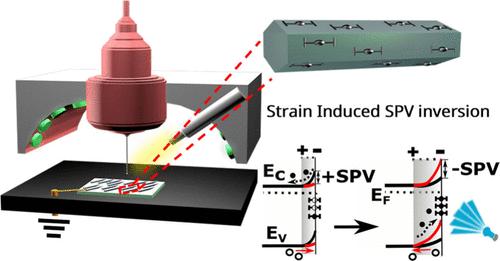
纳米线表面是特别感兴趣的,主要是因为它们在光电应用中的潜力。因此,采用不同的表面处理方法来控制表面效应。在这里,我们成功地将n型氮化镓纳米棒中的n型表面态转移到挑战区(即蓝色区)的p型态。这是通过由表面应变引起的静电场驱动的反向电荷转移实现的。在n型GaN纳米棒中,p型表面态表现出倒置的光电压机制,以及室温下稳定的蓝色光致发光。通过x射线光电子能谱(XPS)、表面光电压、开尔文探针、拉曼和光致发光测量来确定GaN纳米棒阵列表面的反向电荷转移。该机制和研究结论得到了实验和理论的支持。这种表面态反转方法为低维纳米材料中p-n结的调控提供了一种新的策略。
本文章由计算机程序翻译,如有差异,请以英文原文为准。

p-Type Surface Defects on n-GaN Nanorods

p-Type Surface Defects on n-GaN Nanorods
Nanowire surfaces are of particular interest, primarily for their potential in optoelectronic applications. Thus, different surface treatments have been performed to develop methods for controlling the surface effect. Here, we successfully shifted the n-type surface states in n-type GaN nanorods to p-type states in the challenging regime, i.e., the blue regime. This was achieved through reverse charge transfer driven by an electrostatic field induced by surface strain. The p-type surface state demonstrates an inverted photovoltage mechanism, as well as a stable blue photoluminescence at room temperature under ambient conditions, within the n-type GaN nanorods. The inverted charge transfer at the surface of the GaN nanorod array was determined by X-ray photoelectron spectroscopy (XPS), surface photovoltage, Kelvin probe, Raman, and photoluminescence measurements. The mechanism and the study’s conclusions have been supported experimentally and theoretically. This surface state inversion approach offers a new strategy for regulating p–n junctions in low-dimensional nanomaterials.
求助全文
通过发布文献求助,成功后即可免费获取论文全文。 去求助
来源期刊
Nano Letters
Nano Letters 工程技术-材料科学:综合
CiteScore
16.80
自引率
2.80%
发文量
1182
审稿时长
1.4 months
期刊介绍: Nano Letters serves as a dynamic platform for promptly disseminating original results in fundamental, applied, and emerging research across all facets of nanoscience and nanotechnology. A pivotal criterion for inclusion within Nano Letters is the convergence of at least two different areas or disciplines, ensuring a rich interdisciplinary scope. The journal is dedicated to fostering exploration in diverse areas, including: - Experimental and theoretical findings on physical, chemical, and biological phenomena at the nanoscale - Synthesis, characterization, and processing of organic, inorganic, polymer, and hybrid nanomaterials through physical, chemical, and biological methodologies - Modeling and simulation of synthetic, assembly, and interaction processes - Realization of integrated nanostructures and nano-engineered devices exhibiting advanced performance - Applications of nanoscale materials in living and environmental systems Nano Letters is committed to advancing and showcasing groundbreaking research that intersects various domains, fostering innovation and collaboration in the ever-evolving field of nanoscience and nanotechnology.
×
引用
GB/T 7714-2015
复制
MLA
复制
APA
复制
导出至
BibTeX EndNote RefMan NoteFirst NoteExpress
×
提示
您的信息不完整,为了账户安全,请先补充。
现在去补充
×
提示
您因"违规操作"
具体请查看互助需知
我知道了
×
提示
确定
请完成安全验证×
copy
已复制链接
快去分享给好友吧!
我知道了
右上角分享
点击右上角分享
0
联系我们:info@booksci.cn Book学术提供免费学术资源搜索服务,方便国内外学者检索中英文文献。致力于提供最便捷和优质的服务体验。 Copyright © 2023 布克学术 All rights reserved.
京ICP备2023020795号-1
ghs 京公网安备 11010802042870号
Book学术文献互助
Book学术文献互助群
群 号:604180095
Book学术官方微信