Honey Sharma, Shrestha Bhattacharya, Shahnawaz Alam, Silajit Manna, Ashutosh Pandey, Son Pal Singh, Vamsi Krishna Komarala
{"title":"添加剂辅助织构对硅异质结太阳能电池表面形貌和界面缺陷密度的影响","authors":"Honey Sharma, Shrestha Bhattacharya, Shahnawaz Alam, Silajit Manna, Ashutosh Pandey, Son Pal Singh, Vamsi Krishna Komarala","doi":"10.1007/s00339-025-08589-6","DOIUrl":null,"url":null,"abstract":"<div><p>The efficiency of silicon heterojunction (SHJ) solar cells depends critically on c-Si surface topography and defect passivation. This study optimizes the formation of random pyramids using chemical additives in the texturization solution, achieving pyramids with optimal base and vertex angles and a low surface reflectance of ∼ 10.51%. Interface defect states (D<sub>it</sub>) and surface lifetime (τ<sub>surf</sub>) were analysed at various cell fabrication stages. The deposition of i-a-Si: H layers on both sides of the textured wafer reduced D<sub>it</sub> to ∼ 8.5 × 10<sup>8</sup> eV<sup>− 1</sup>cm<sup>− 2</sup> with τ<sub>surf</sub> ∼ 4.9 ms indicating good chemical passivation of the defects. Adding the carrier-selective layers (p-a-Si: H and n-nc-Si: H) further reduced D<sub>it</sub> to ∼ 7.0 × 10<sup>8</sup> eV<sup>− 1</sup>cm<sup>− 2</sup> and enhanced τ<sub>surf</sub> to ∼ 21.0 ms. However, sputtering-induced plasma damage during ITO deposition increased D<sub>it</sub> to ∼ 11.8 × 10<sup>8</sup> eV<sup>− 1</sup>cm<sup>− 2</sup>, lowering τ<sub>surf</sub> to ∼ 3.3 ms. Optimized c-Si surface conditioning led to a power conversion efficiency of ∼ 22.4% and an open-circuit voltage of ∼ 727 mV from an SHJ cell. Device dark current-voltage analysis also provided insights into the charge carrier recombination dynamics.</p></div>","PeriodicalId":473,"journal":{"name":"Applied Physics A","volume":"131 6","pages":""},"PeriodicalIF":2.8000,"publicationDate":"2025-05-16","publicationTypes":"Journal Article","fieldsOfStudy":null,"isOpenAccess":false,"openAccessPdf":"","citationCount":"0","resultStr":"{\"title\":\"Role of additive-assisted texturing on surface morphology and interface defect density in silicon heterojunction solar cells\",\"authors\":\"Honey Sharma, Shrestha Bhattacharya, Shahnawaz Alam, Silajit Manna, Ashutosh Pandey, Son Pal Singh, Vamsi Krishna Komarala\",\"doi\":\"10.1007/s00339-025-08589-6\",\"DOIUrl\":null,\"url\":null,\"abstract\":\"<div><p>The efficiency of silicon heterojunction (SHJ) solar cells depends critically on c-Si surface topography and defect passivation. This study optimizes the formation of random pyramids using chemical additives in the texturization solution, achieving pyramids with optimal base and vertex angles and a low surface reflectance of ∼ 10.51%. Interface defect states (D<sub>it</sub>) and surface lifetime (τ<sub>surf</sub>) were analysed at various cell fabrication stages. The deposition of i-a-Si: H layers on both sides of the textured wafer reduced D<sub>it</sub> to ∼ 8.5 × 10<sup>8</sup> eV<sup>− 1</sup>cm<sup>− 2</sup> with τ<sub>surf</sub> ∼ 4.9 ms indicating good chemical passivation of the defects. Adding the carrier-selective layers (p-a-Si: H and n-nc-Si: H) further reduced D<sub>it</sub> to ∼ 7.0 × 10<sup>8</sup> eV<sup>− 1</sup>cm<sup>− 2</sup> and enhanced τ<sub>surf</sub> to ∼ 21.0 ms. However, sputtering-induced plasma damage during ITO deposition increased D<sub>it</sub> to ∼ 11.8 × 10<sup>8</sup> eV<sup>− 1</sup>cm<sup>− 2</sup>, lowering τ<sub>surf</sub> to ∼ 3.3 ms. Optimized c-Si surface conditioning led to a power conversion efficiency of ∼ 22.4% and an open-circuit voltage of ∼ 727 mV from an SHJ cell. Device dark current-voltage analysis also provided insights into the charge carrier recombination dynamics.</p></div>\",\"PeriodicalId\":473,\"journal\":{\"name\":\"Applied Physics A\",\"volume\":\"131 6\",\"pages\":\"\"},\"PeriodicalIF\":2.8000,\"publicationDate\":\"2025-05-16\",\"publicationTypes\":\"Journal Article\",\"fieldsOfStudy\":null,\"isOpenAccess\":false,\"openAccessPdf\":\"\",\"citationCount\":\"0\",\"resultStr\":null,\"platform\":\"Semanticscholar\",\"paperid\":null,\"PeriodicalName\":\"Applied Physics A\",\"FirstCategoryId\":\"4\",\"ListUrlMain\":\"https://link.springer.com/article/10.1007/s00339-025-08589-6\",\"RegionNum\":4,\"RegionCategory\":\"材料科学\",\"ArticlePicture\":[],\"TitleCN\":null,\"AbstractTextCN\":null,\"PMCID\":null,\"EPubDate\":\"\",\"PubModel\":\"\",\"JCR\":\"Q3\",\"JCRName\":\"MATERIALS SCIENCE, MULTIDISCIPLINARY\",\"Score\":null,\"Total\":0}","platform":"Semanticscholar","paperid":null,"PeriodicalName":"Applied Physics A","FirstCategoryId":"4","ListUrlMain":"https://link.springer.com/article/10.1007/s00339-025-08589-6","RegionNum":4,"RegionCategory":"材料科学","ArticlePicture":[],"TitleCN":null,"AbstractTextCN":null,"PMCID":null,"EPubDate":"","PubModel":"","JCR":"Q3","JCRName":"MATERIALS SCIENCE, MULTIDISCIPLINARY","Score":null,"Total":0}
Role of additive-assisted texturing on surface morphology and interface defect density in silicon heterojunction solar cells
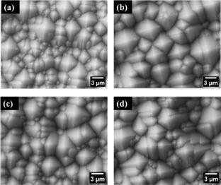
The efficiency of silicon heterojunction (SHJ) solar cells depends critically on c-Si surface topography and defect passivation. This study optimizes the formation of random pyramids using chemical additives in the texturization solution, achieving pyramids with optimal base and vertex angles and a low surface reflectance of ∼ 10.51%. Interface defect states (Dit) and surface lifetime (τsurf) were analysed at various cell fabrication stages. The deposition of i-a-Si: H layers on both sides of the textured wafer reduced Dit to ∼ 8.5 × 10⁸ eV− 1cm− 2 with τsurf ∼ 4.9 ms indicating good chemical passivation of the defects. Adding the carrier-selective layers (p-a-Si: H and n-nc-Si: H) further reduced Dit to ∼ 7.0 × 10⁸ eV− 1cm− 2 and enhanced τsurf to ∼ 21.0 ms. However, sputtering-induced plasma damage during ITO deposition increased Dit to ∼ 11.8 × 10⁸ eV− 1cm− 2, lowering τsurf to ∼ 3.3 ms. Optimized c-Si surface conditioning led to a power conversion efficiency of ∼ 22.4% and an open-circuit voltage of ∼ 727 mV from an SHJ cell. Device dark current-voltage analysis also provided insights into the charge carrier recombination dynamics.
期刊介绍:
Applied Physics A publishes experimental and theoretical investigations in applied physics as regular articles, rapid communications, and invited papers. The distinguished 30-member Board of Editors reflects the interdisciplinary approach of the journal and ensures the highest quality of peer review.
 求助内容:
求助内容: 应助结果提醒方式:


