基于CuI纳米晶修饰CdSe纳米带的原位高性能光电探测器

IF 8.2 2区 材料科学 Q1 MATERIALS SCIENCE, MULTIDISCIPLINARY
Dachen Yang, Haoran Sheng, Guo Li, Honglai Li, Yipeng Zhao, Zhiqiang Li, Liang Ma, Yicheng Wang, Dengyu Zhang
{"title":"基于CuI纳米晶修饰CdSe纳米带的原位高性能光电探测器","authors":"Dachen Yang, Haoran Sheng, Guo Li, Honglai Li, Yipeng Zhao, Zhiqiang Li, Liang Ma, Yicheng Wang, Dengyu Zhang","doi":"10.1021/acsami.5c01910","DOIUrl":null,"url":null,"abstract":"Photodetectors with high responsivity are crucial elements in various modern industrial applications. CdSe nanobelts, due to their direct bandgap, have emerged as a high-performance material with wide-ranging applications in photodetector technology. For CdSe nanobelt-based photodetectors, which already exhibit broad applicability, enhancing their performance is a key area of ongoing research and development. In this study, we report the successful synthesis of CdSe nanobelt photodetectors decorated with CuI nanocrystals through a combination of physical vapor deposition and a poly(vinyl alcohol) film transfer process. This approach significantly improves the performance of the photodetectors. In the 405–765 nm range with fixed light intensity, the responsivity and external quantum efficiency of the CuI@CdSe photodetectors peaked at 242.88 A/W and 579.18%, 11.6 times higher than those of the in-situ CdSe photodetectors. At 520 nm with 0.94 mW/cm<sup>2</sup> intensity, these metrics reached 289.53 A/W and 860.727%, about 38.645 times higher than those of the in-situ CdSe photodetectors. To further demonstrate the enhanced performance, we prepared an image signal transmission system to validate the optical imaging capabilities of the photodetectors. The CuI@CdSe photodetectors successfully converted a preset image into the final output image with a resolution of 110 × 93 pixels, showcasing their potential for practical imaging applications. This work significantly boosts the responsivity and external quantum efficiency of CdSe photodetectors through the incorporation of CuI nanocrystals. It also paves the way toward creating advanced high-performance photodetectors of the future.","PeriodicalId":5,"journal":{"name":"ACS Applied Materials & Interfaces","volume":"6 1","pages":""},"PeriodicalIF":8.2000,"publicationDate":"2025-05-09","publicationTypes":"Journal Article","fieldsOfStudy":null,"isOpenAccess":false,"openAccessPdf":"","citationCount":"0","resultStr":"{\"title\":\"In-Situ High-Performance Photodetectors Based on CdSe Nanobelts Decorated with CuI Nanocrystals\",\"authors\":\"Dachen Yang, Haoran Sheng, Guo Li, Honglai Li, Yipeng Zhao, Zhiqiang Li, Liang Ma, Yicheng Wang, Dengyu Zhang\",\"doi\":\"10.1021/acsami.5c01910\",\"DOIUrl\":null,\"url\":null,\"abstract\":\"Photodetectors with high responsivity are crucial elements in various modern industrial applications. CdSe nanobelts, due to their direct bandgap, have emerged as a high-performance material with wide-ranging applications in photodetector technology. For CdSe nanobelt-based photodetectors, which already exhibit broad applicability, enhancing their performance is a key area of ongoing research and development. In this study, we report the successful synthesis of CdSe nanobelt photodetectors decorated with CuI nanocrystals through a combination of physical vapor deposition and a poly(vinyl alcohol) film transfer process. This approach significantly improves the performance of the photodetectors. In the 405–765 nm range with fixed light intensity, the responsivity and external quantum efficiency of the CuI@CdSe photodetectors peaked at 242.88 A/W and 579.18%, 11.6 times higher than those of the in-situ CdSe photodetectors. At 520 nm with 0.94 mW/cm<sup>2</sup> intensity, these metrics reached 289.53 A/W and 860.727%, about 38.645 times higher than those of the in-situ CdSe photodetectors. To further demonstrate the enhanced performance, we prepared an image signal transmission system to validate the optical imaging capabilities of the photodetectors. The CuI@CdSe photodetectors successfully converted a preset image into the final output image with a resolution of 110 × 93 pixels, showcasing their potential for practical imaging applications. This work significantly boosts the responsivity and external quantum efficiency of CdSe photodetectors through the incorporation of CuI nanocrystals. It also paves the way toward creating advanced high-performance photodetectors of the future.\",\"PeriodicalId\":5,\"journal\":{\"name\":\"ACS Applied Materials & Interfaces\",\"volume\":\"6 1\",\"pages\":\"\"},\"PeriodicalIF\":8.2000,\"publicationDate\":\"2025-05-09\",\"publicationTypes\":\"Journal Article\",\"fieldsOfStudy\":null,\"isOpenAccess\":false,\"openAccessPdf\":\"\",\"citationCount\":\"0\",\"resultStr\":null,\"platform\":\"Semanticscholar\",\"paperid\":null,\"PeriodicalName\":\"ACS Applied Materials & Interfaces\",\"FirstCategoryId\":\"88\",\"ListUrlMain\":\"https://doi.org/10.1021/acsami.5c01910\",\"RegionNum\":2,\"RegionCategory\":\"材料科学\",\"ArticlePicture\":[],\"TitleCN\":null,\"AbstractTextCN\":null,\"PMCID\":null,\"EPubDate\":\"\",\"PubModel\":\"\",\"JCR\":\"Q1\",\"JCRName\":\"MATERIALS SCIENCE, MULTIDISCIPLINARY\",\"Score\":null,\"Total\":0}","platform":"Semanticscholar","paperid":null,"PeriodicalName":"ACS Applied Materials & Interfaces","FirstCategoryId":"88","ListUrlMain":"https://doi.org/10.1021/acsami.5c01910","RegionNum":2,"RegionCategory":"材料科学","ArticlePicture":[],"TitleCN":null,"AbstractTextCN":null,"PMCID":null,"EPubDate":"","PubModel":"","JCR":"Q1","JCRName":"MATERIALS SCIENCE, MULTIDISCIPLINARY","Score":null,"Total":0}
引用次数: 0

摘要

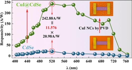
具有高响应性的光电探测器是现代工业应用的重要组成部分。CdSe纳米带由于其直接带隙特性,已成为一种高性能材料,在光电探测器技术中有着广泛的应用。对于已经表现出广泛适用性的CdSe纳米带光电探测器来说,提高其性能是正在进行的研究和开发的关键领域。在这项研究中,我们报道了通过物理气相沉积和聚乙烯醇薄膜转移工艺的结合,成功合成了用CuI纳米晶体装饰的CdSe纳米带光电探测器。这种方法显著提高了光电探测器的性能。在固定光强的405 ~ 765 nm范围内,CuI@CdSe光电探测器的响应率和外量子效率分别达到242.88 A/W和579.18%,是原位CdSe光电探测器的11.6倍。在520nm强度为0.94 mW/cm2时,这些指标达到289.53 A/W和860.727%,是原位CdSe光电探测器的38.645倍。为了进一步证明增强的性能,我们准备了一个图像信号传输系统来验证光电探测器的光学成像能力。CuI@CdSe光电探测器成功地将预设图像转换为最终输出图像,分辨率为110 × 93像素,展示了它们在实际成像应用中的潜力。本工作通过加入CuI纳米晶体,显著提高了CdSe光电探测器的响应率和外量子效率。它也为创造未来先进的高性能光电探测器铺平了道路。
本文章由计算机程序翻译,如有差异,请以英文原文为准。

In-Situ High-Performance Photodetectors Based on CdSe Nanobelts Decorated with CuI Nanocrystals

In-Situ High-Performance Photodetectors Based on CdSe Nanobelts Decorated with CuI Nanocrystals
Photodetectors with high responsivity are crucial elements in various modern industrial applications. CdSe nanobelts, due to their direct bandgap, have emerged as a high-performance material with wide-ranging applications in photodetector technology. For CdSe nanobelt-based photodetectors, which already exhibit broad applicability, enhancing their performance is a key area of ongoing research and development. In this study, we report the successful synthesis of CdSe nanobelt photodetectors decorated with CuI nanocrystals through a combination of physical vapor deposition and a poly(vinyl alcohol) film transfer process. This approach significantly improves the performance of the photodetectors. In the 405–765 nm range with fixed light intensity, the responsivity and external quantum efficiency of the CuI@CdSe photodetectors peaked at 242.88 A/W and 579.18%, 11.6 times higher than those of the in-situ CdSe photodetectors. At 520 nm with 0.94 mW/cm2 intensity, these metrics reached 289.53 A/W and 860.727%, about 38.645 times higher than those of the in-situ CdSe photodetectors. To further demonstrate the enhanced performance, we prepared an image signal transmission system to validate the optical imaging capabilities of the photodetectors. The CuI@CdSe photodetectors successfully converted a preset image into the final output image with a resolution of 110 × 93 pixels, showcasing their potential for practical imaging applications. This work significantly boosts the responsivity and external quantum efficiency of CdSe photodetectors through the incorporation of CuI nanocrystals. It also paves the way toward creating advanced high-performance photodetectors of the future.
求助全文
通过发布文献求助,成功后即可免费获取论文全文。 去求助
来源期刊
ACS Applied Materials & Interfaces
ACS Applied Materials & Interfaces 工程技术-材料科学:综合
CiteScore
16.00
自引率
6.30%
发文量
4978
审稿时长
1.8 months
期刊介绍: ACS Applied Materials & Interfaces is a leading interdisciplinary journal that brings together chemists, engineers, physicists, and biologists to explore the development and utilization of newly-discovered materials and interfacial processes for specific applications. Our journal has experienced remarkable growth since its establishment in 2009, both in terms of the number of articles published and the impact of the research showcased. We are proud to foster a truly global community, with the majority of published articles originating from outside the United States, reflecting the rapid growth of applied research worldwide.
×
引用
GB/T 7714-2015
复制
MLA
复制
APA
复制
导出至
BibTeX EndNote RefMan NoteFirst NoteExpress
×
提示
您的信息不完整,为了账户安全,请先补充。
现在去补充
×
提示
您因"违规操作"
具体请查看互助需知
我知道了
×
提示
确定
请完成安全验证×
copy
已复制链接
快去分享给好友吧!
我知道了
右上角分享
点击右上角分享
0
联系我们:info@booksci.cn Book学术提供免费学术资源搜索服务,方便国内外学者检索中英文文献。致力于提供最便捷和优质的服务体验。 Copyright © 2023 布克学术 All rights reserved.
京ICP备2023020795号-1
ghs 京公网安备 11010802042870号
Book学术文献互助
Book学术文献互助群
群 号:604180095
Book学术官方微信