六英寸高纯度铅卤化钙钛矿晶圆源自陶瓷制造技术
IF 19
1区 材料科学
Q1 CHEMISTRY, MULTIDISCIPLINARY
引用次数: 0
摘要
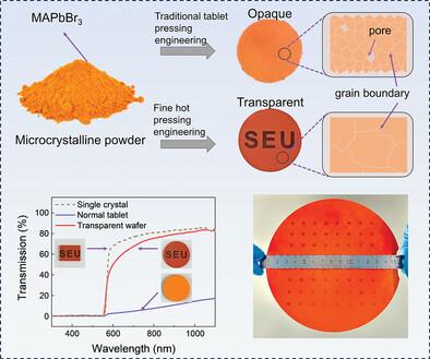
卤化铅钙钛矿具有优异的光电性能,但由于无法制造大面积、高质量的晶圆而面临产业化障碍。受陶瓷制造技术的启发,开发了6英寸高纯度钙钛矿晶片,实现了与单晶相当的载流子迁移率,寿命和缺陷浓度。该方法证明了不同钙钛矿的通用性,并实现了异质结晶圆,标志着载流子动力学控制的重大进展。利用10 × 10 cm2的钙钛矿异质结硅片构建了256 × 256像素的x射线传感阵列,其灵敏度为36532µCGyair−1 cm−2,检测限为139 nGyair s−1,优于单晶探测器(10640µCGyair−1 cm−2和247 nGyair s−1)。这一突破为工业规模的钙钛矿光电子技术建立了一条可扩展的途径,克服了关键的制造障碍,同时通过晶片级异质结构工程实现了高性能辐射成像系统。本文章由计算机程序翻译,如有差异,请以英文原文为准。
Six-Inch High-Purity Lead Halide Perovskite Wafer Derived from Ceramic Manufacturing Technique
Lead halide perovskites exhibit exceptional optoelectronic properties but face industrialization barriers due to the inability to fabricate large-area, high-quality wafers. Inspired by ceramic manufacturing techniques, a 6-inch high-purity perovskite wafer is developed, achieving carrier mobility, lifetime, and defect concentrations comparable to single crystals. This method demonstrates universality across diverse perovskites and enables heterojunction wafers, marking significant progress in carrier dynamics control. As a result, an X-ray sensing array with 256 × 256 pixels is constructed using a 10 × 10 cm2 perovskite heterojunction wafer, which exhibits a sensitivity of 36532 µCGyair−1 cm−2 and a low detection limit of 139 nGyair s−1, superior to those in a single-crystal detector (10640 µCGyair−1 cm−2 and 247 nGyair s−1). This breakthrough establishes a scalable pathway to industrial-scale perovskite optoelectronics, overcoming critical manufacturing barriers while enabling high-performance radiation imaging systems through wafer-level heterostructure engineering.
求助全文
通过发布文献求助,成功后即可免费获取论文全文。
去求助
来源期刊
Advanced Functional Materials
工程技术-材料科学:综合
CiteScore
29.50
自引率
4.20%
发文量
2086
审稿时长
2.1 months
期刊介绍:
Firmly established as a top-tier materials science journal, Advanced Functional Materials reports breakthrough research in all aspects of materials science, including nanotechnology, chemistry, physics, and biology every week.
Advanced Functional Materials is known for its rapid and fair peer review, quality content, and high impact, making it the first choice of the international materials science community.
 求助内容:
求助内容: 应助结果提醒方式:


