Ga2O3同外延薄膜中纳米级旋转晶体的原子界面结构和电子特性
IF 6.9
2区 材料科学
Q2 CHEMISTRY, PHYSICAL
引用次数: 0
摘要
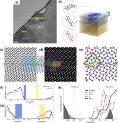
虽然β-Ga2O3正在成为下一代电力电子材料,但由于其复杂的晶体结构,对二维缺陷的理解仍然缺乏。本文报道了β-Ga2O3同外延层的纳米级旋转晶体,并鉴定了其晶体结构和电子性能。通过扫描透射电子显微镜和密度泛函理论计算,我们分析了晶体取向为(2¯2¯01)旋转//(202)矩阵和[010]旋转//[010]矩阵的同外延薄膜中的旋转晶体。(2¯2¯01)//(202)界面处的失配小至0.0013,非常接近于零。亚纳米尺度的特定Ga原子位移为 ~ 1.03 Å,在界面处反复、规律地出现。通过DFT计算得到界面形成能为75.3 mJ/m2,这与半导体材料的层错能相比是非常小的。此外,该缺陷本身引起了离域深能级态,我们进一步通过边界处的杂质偏析计算了带结构的变化,这些变化很难被杂质偏析钝化。这些结果对局部形成的纳米级缺陷的原子尺度界面结构及其电子性质提供了基本的认识。本文章由计算机程序翻译,如有差异,请以英文原文为准。

Atomic interface structure and electronic properties at nanoscale rotated crystal in Ga2O3 homoepitaxial film
Although β-Ga2O3 is emerging as a next-generation power-electronics material, the understanding of two-dimensional defects is still lacking due to its complex crystal structure. We report a nanoscale rotated crystal of the β-Ga2O3 homoepitaxial layer and identify its crystal structure and electronic properties. By coordinating scanning transmission electron microscopy and density functional theory calculations, we analyze the rotated crystal in the homoepitaxial film with a crystallographic orientation of (01)rotated//(202)matrix and [010]rotated//[010]matrix. The mismatch at the (01)//(202) interface was as small as 0.0013, which is very close to zero. Sub-nanometer scale displacement of specific Ga atoms by ∼ 1.03 Å, appearing repeatedly and regularly at the interface was found. From DFT calculation the interface formation energy was determined to be 75.3 mJ/m2, which is very small compared to stacking fault energy of semiconductor materials. In addition, this defect itself induces delocalized deep-level states and we further calculated changes in band structure by impurity segregation at the boundary, which are difficult to passivate with segregation of impurities. These results provide a fundamental understanding into the atomic-scale interfacial structure at the locally formed nanoscale defect and their electronic property.
求助全文
通过发布文献求助,成功后即可免费获取论文全文。
去求助
来源期刊

Applied Surface Science
工程技术-材料科学:膜
CiteScore
12.50
自引率
7.50%
发文量
3393
审稿时长
67 days
期刊介绍:
Applied Surface Science covers topics contributing to a better understanding of surfaces, interfaces, nanostructures and their applications. The journal is concerned with scientific research on the atomic and molecular level of material properties determined with specific surface analytical techniques and/or computational methods, as well as the processing of such structures.
 求助内容:
求助内容: 应助结果提醒方式:


