Yue Cheng, Rui Xin, Li Yu, Feiyu Mao, Xiang Li, Wenjuan Wang and Tianxin Li
{"title":"InGaAs/InP雪崩光电二极管中的光载流子分布及其对器件性能的贡献","authors":"Yue Cheng, Rui Xin, Li Yu, Feiyu Mao, Xiang Li, Wenjuan Wang and Tianxin Li","doi":"10.1039/D5NR00600G","DOIUrl":null,"url":null,"abstract":"<p >The InGaAs/InP avalanche photodiode (APD) is one of the best single photon detectors in the near-infrared wavelength range. To approach its optimal performance, it would be helpful to reveal the electrical and photoelectric properties within its core regions from a microscopic perspective. Herein, we employed cross-sectional scanning capacitance microscopy (SCM) to investigate the photocarrier behaviors in two APD devices under excitation of different light wavelengths. The grading and charge layers as well as the multiplication regions of the APDs were well resolved electrically in this study. The light-induced capacitance response in the multiplication region was found to differ by 2–4 times in the two devices, signifying a much higher photocarrier concentration under the same excitation intensity. Additionally, a sharp gradient of capacitance was observed along the core regions, which directly reflects the pronounced drifting of photocarriers in the strong built-in electric field. The findings of this study substantiate the low dark current and high gain merits of the APD device, providing an effective strategy to explore the spatial and physical origin of the device performance through nanoscopic observation of carriers in the active area.</p>","PeriodicalId":92,"journal":{"name":"Nanoscale","volume":" 32","pages":" 18727-18734"},"PeriodicalIF":5.1000,"publicationDate":"2025-05-08","publicationTypes":"Journal Article","fieldsOfStudy":null,"isOpenAccess":false,"openAccessPdf":"","citationCount":"0","resultStr":"{\"title\":\"Photocarrier distribution in InGaAs/InP avalanche photodiodes and its contribution to device performances\",\"authors\":\"Yue Cheng, Rui Xin, Li Yu, Feiyu Mao, Xiang Li, Wenjuan Wang and Tianxin Li\",\"doi\":\"10.1039/D5NR00600G\",\"DOIUrl\":null,\"url\":null,\"abstract\":\"<p >The InGaAs/InP avalanche photodiode (APD) is one of the best single photon detectors in the near-infrared wavelength range. To approach its optimal performance, it would be helpful to reveal the electrical and photoelectric properties within its core regions from a microscopic perspective. Herein, we employed cross-sectional scanning capacitance microscopy (SCM) to investigate the photocarrier behaviors in two APD devices under excitation of different light wavelengths. The grading and charge layers as well as the multiplication regions of the APDs were well resolved electrically in this study. The light-induced capacitance response in the multiplication region was found to differ by 2–4 times in the two devices, signifying a much higher photocarrier concentration under the same excitation intensity. Additionally, a sharp gradient of capacitance was observed along the core regions, which directly reflects the pronounced drifting of photocarriers in the strong built-in electric field. The findings of this study substantiate the low dark current and high gain merits of the APD device, providing an effective strategy to explore the spatial and physical origin of the device performance through nanoscopic observation of carriers in the active area.</p>\",\"PeriodicalId\":92,\"journal\":{\"name\":\"Nanoscale\",\"volume\":\" 32\",\"pages\":\" 18727-18734\"},\"PeriodicalIF\":5.1000,\"publicationDate\":\"2025-05-08\",\"publicationTypes\":\"Journal Article\",\"fieldsOfStudy\":null,\"isOpenAccess\":false,\"openAccessPdf\":\"\",\"citationCount\":\"0\",\"resultStr\":null,\"platform\":\"Semanticscholar\",\"paperid\":null,\"PeriodicalName\":\"Nanoscale\",\"FirstCategoryId\":\"88\",\"ListUrlMain\":\"https://pubs.rsc.org/en/content/articlelanding/2025/nr/d5nr00600g\",\"RegionNum\":3,\"RegionCategory\":\"材料科学\",\"ArticlePicture\":[],\"TitleCN\":null,\"AbstractTextCN\":null,\"PMCID\":null,\"EPubDate\":\"\",\"PubModel\":\"\",\"JCR\":\"Q1\",\"JCRName\":\"CHEMISTRY, MULTIDISCIPLINARY\",\"Score\":null,\"Total\":0}","platform":"Semanticscholar","paperid":null,"PeriodicalName":"Nanoscale","FirstCategoryId":"88","ListUrlMain":"https://pubs.rsc.org/en/content/articlelanding/2025/nr/d5nr00600g","RegionNum":3,"RegionCategory":"材料科学","ArticlePicture":[],"TitleCN":null,"AbstractTextCN":null,"PMCID":null,"EPubDate":"","PubModel":"","JCR":"Q1","JCRName":"CHEMISTRY, MULTIDISCIPLINARY","Score":null,"Total":0}
Photocarrier distribution in InGaAs/InP avalanche photodiodes and its contribution to device performances
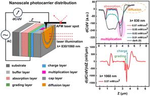
The InGaAs/InP avalanche photodiode (APD) is one of the best single photon detectors in the near-infrared wavelength range. To approach its optimal performance, it would be helpful to reveal the electrical and photoelectric properties within its core regions from a microscopic perspective. Herein, we employed cross-sectional scanning capacitance microscopy (SCM) to investigate the photocarrier behaviors in two APD devices under excitation of different light wavelengths. The grading and charge layers as well as the multiplication regions of the APDs were well resolved electrically in this study. The light-induced capacitance response in the multiplication region was found to differ by 2–4 times in the two devices, signifying a much higher photocarrier concentration under the same excitation intensity. Additionally, a sharp gradient of capacitance was observed along the core regions, which directly reflects the pronounced drifting of photocarriers in the strong built-in electric field. The findings of this study substantiate the low dark current and high gain merits of the APD device, providing an effective strategy to explore the spatial and physical origin of the device performance through nanoscopic observation of carriers in the active area.
期刊介绍:
Nanoscale is a high-impact international journal, publishing high-quality research across nanoscience and nanotechnology. Nanoscale publishes a full mix of research articles on experimental and theoretical work, including reviews, communications, and full papers.Highly interdisciplinary, this journal appeals to scientists, researchers and professionals interested in nanoscience and nanotechnology, quantum materials and quantum technology, including the areas of physics, chemistry, biology, medicine, materials, energy/environment, information technology, detection science, healthcare and drug discovery, and electronics.


 求助内容:
求助内容: 应助结果提醒方式:


