法拉第光刻
IF 9.1
1区 材料科学
Q1 CHEMISTRY, MULTIDISCIPLINARY
引用次数: 0
摘要
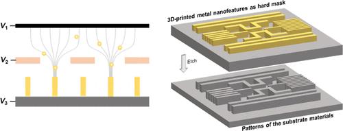
随着摩尔定律继续推动集成电路的临界尺寸(CD)缩放,传统光刻技术接近基本分辨率极限。虽然自对齐双模式和定向自组装等替代策略解决了这些挑战,但它们引入了工艺复杂性和制造可变性。在这里,我们开发了法拉第光刻(FL),这是一种将纳米级3D打印与传统纳米制造相结合的新方法,以克服这些限制。在保持工艺简单性的同时,FL在原子尺度精度(0.95 nm线边缘粗糙度)和优异的局部CD均匀性方面实现了卓越的35 nm特征。该技术展示了在不同基材上进行2D/3D图案的独特能力,其导电性或透明度没有影响。与现有方法不同,FL无需额外的工艺步骤或复杂的材料要求即可实现这一目标。这种高分辨率、3D能力和材料多功能性的结合,使FL既成为当前图形技术的有价值的补充,又成为半导体纳米制造创新的潜在催化剂。本文章由计算机程序翻译,如有差异,请以英文原文为准。
Faraday Lithography
As Moore’s Law continues to push critical dimension (CD) scaling in integrated circuits, conventional photolithography approaches fundamental resolution limits. While alternative strategies such as self-aligned double patterning and directed self-assembly address these challenges, they introduce process complexity and manufacturing variability. Here we develop Faraday lithography (FL), a novel approach that hybridizes nanoscale 3D printing with conventional nanofabrication to overcome these limitations. FL achieves remarkable 35 nm features with atomic-scale precision (0.95 nm line edge roughness) and excellent local CD uniformity while maintaining process simplicity. The technique demonstrates unique capabilities for 2D/3D patterning across diverse substrates, whose conductivity or transparency has no influence. Unlike existing methods, FL accomplishes this without additional process steps or complex material requirements. This combination of high resolution, 3D capability, and material versatility positions FL as both a valuable complement to current patterning technologies and a potential catalyst for semiconductor nanomanufacturing innovation.
求助全文
通过发布文献求助,成功后即可免费获取论文全文。
去求助
来源期刊

Nano Letters
工程技术-材料科学:综合
CiteScore
16.80
自引率
2.80%
发文量
1182
审稿时长
1.4 months
期刊介绍:
Nano Letters serves as a dynamic platform for promptly disseminating original results in fundamental, applied, and emerging research across all facets of nanoscience and nanotechnology. A pivotal criterion for inclusion within Nano Letters is the convergence of at least two different areas or disciplines, ensuring a rich interdisciplinary scope. The journal is dedicated to fostering exploration in diverse areas, including:
- Experimental and theoretical findings on physical, chemical, and biological phenomena at the nanoscale
- Synthesis, characterization, and processing of organic, inorganic, polymer, and hybrid nanomaterials through physical, chemical, and biological methodologies
- Modeling and simulation of synthetic, assembly, and interaction processes
- Realization of integrated nanostructures and nano-engineered devices exhibiting advanced performance
- Applications of nanoscale materials in living and environmental systems
Nano Letters is committed to advancing and showcasing groundbreaking research that intersects various domains, fostering innovation and collaboration in the ever-evolving field of nanoscience and nanotechnology.
 求助内容:
求助内容: 应助结果提醒方式:


