高质量p型触点,用于高工作功能半金属TiS2电极的原子薄MoTe2晶体管

IF 8.2 2区 材料科学 Q1 MATERIALS SCIENCE, MULTIDISCIPLINARY
Boyuan Di, Xinlu Li, Xiaokun Wen, Wenyu Lei, Xinyue Xu, Wenchao Kong, Haixin Chang, Jia Zhang, Wenfeng Zhang
{"title":"高质量p型触点,用于高工作功能半金属TiS2电极的原子薄MoTe2晶体管","authors":"Boyuan Di, Xinlu Li, Xiaokun Wen, Wenyu Lei, Xinyue Xu, Wenchao Kong, Haixin Chang, Jia Zhang, Wenfeng Zhang","doi":"10.1021/acsami.5c04059","DOIUrl":null,"url":null,"abstract":"High-performance p-type atomically thin transistors are fundamental components in CMOS-based digital logic circuits for beyond-silicon electronics. Compared with the recent breakthrough in high-quality semimetal contacts approaching the quantum limit on n-type atomically thin channel transistors, achieving high-performance p-type analogues with high-quality contacts remains challenging, which was mainly hindered by the lack of proper high-work-function metallic electrodes with Fermi level unpinning capacity. Herein, we demonstrate that semimetal TiS<sub>2</sub> electrodes prepared with a damage-free transfer process can be a feasible option for p-type atomically thin MoTe<sub>2</sub> transistors. Owing to its intrinsic large work function (∼5.3 eV) and high-quality contacts with negligible Schottky barrier at the TiS<sub>2</sub>/MoTe<sub>2</sub> interface, the scaled p-type bilayer MoTe<sub>2</sub> transistor with 500 nm channel length and the monolayer transistor with 800 nm channel length exhibit a high on-state current (<i>I</i><sub>on</sub>) of 100 μA/μm with the on/off ratio (<i>I</i><sub>on/off</sub>) over 10<sup>6</sup> and an <i>I</i><sub>on</sub> of 68 μA/μm with the <i>I</i><sub>on/off</sub> ratio over 10<sup>7</sup>, respectively. Such a demonstration will enable monolithic atomically thin MoTe<sub>2</sub>-based beyond-silicon electronics via the common CMOS technology.","PeriodicalId":5,"journal":{"name":"ACS Applied Materials & Interfaces","volume":"267 1","pages":""},"PeriodicalIF":8.2000,"publicationDate":"2025-04-18","publicationTypes":"Journal Article","fieldsOfStudy":null,"isOpenAccess":false,"openAccessPdf":"","citationCount":"0","resultStr":"{\"title\":\"High-Quality P-type Contacts for Atomically Thin MoTe2 Transistors with High-Work-Function Semimetal TiS2 Electrodes\",\"authors\":\"Boyuan Di, Xinlu Li, Xiaokun Wen, Wenyu Lei, Xinyue Xu, Wenchao Kong, Haixin Chang, Jia Zhang, Wenfeng Zhang\",\"doi\":\"10.1021/acsami.5c04059\",\"DOIUrl\":null,\"url\":null,\"abstract\":\"High-performance p-type atomically thin transistors are fundamental components in CMOS-based digital logic circuits for beyond-silicon electronics. Compared with the recent breakthrough in high-quality semimetal contacts approaching the quantum limit on n-type atomically thin channel transistors, achieving high-performance p-type analogues with high-quality contacts remains challenging, which was mainly hindered by the lack of proper high-work-function metallic electrodes with Fermi level unpinning capacity. Herein, we demonstrate that semimetal TiS<sub>2</sub> electrodes prepared with a damage-free transfer process can be a feasible option for p-type atomically thin MoTe<sub>2</sub> transistors. Owing to its intrinsic large work function (∼5.3 eV) and high-quality contacts with negligible Schottky barrier at the TiS<sub>2</sub>/MoTe<sub>2</sub> interface, the scaled p-type bilayer MoTe<sub>2</sub> transistor with 500 nm channel length and the monolayer transistor with 800 nm channel length exhibit a high on-state current (<i>I</i><sub>on</sub>) of 100 μA/μm with the on/off ratio (<i>I</i><sub>on/off</sub>) over 10<sup>6</sup> and an <i>I</i><sub>on</sub> of 68 μA/μm with the <i>I</i><sub>on/off</sub> ratio over 10<sup>7</sup>, respectively. Such a demonstration will enable monolithic atomically thin MoTe<sub>2</sub>-based beyond-silicon electronics via the common CMOS technology.\",\"PeriodicalId\":5,\"journal\":{\"name\":\"ACS Applied Materials & Interfaces\",\"volume\":\"267 1\",\"pages\":\"\"},\"PeriodicalIF\":8.2000,\"publicationDate\":\"2025-04-18\",\"publicationTypes\":\"Journal Article\",\"fieldsOfStudy\":null,\"isOpenAccess\":false,\"openAccessPdf\":\"\",\"citationCount\":\"0\",\"resultStr\":null,\"platform\":\"Semanticscholar\",\"paperid\":null,\"PeriodicalName\":\"ACS Applied Materials & Interfaces\",\"FirstCategoryId\":\"88\",\"ListUrlMain\":\"https://doi.org/10.1021/acsami.5c04059\",\"RegionNum\":2,\"RegionCategory\":\"材料科学\",\"ArticlePicture\":[],\"TitleCN\":null,\"AbstractTextCN\":null,\"PMCID\":null,\"EPubDate\":\"\",\"PubModel\":\"\",\"JCR\":\"Q1\",\"JCRName\":\"MATERIALS SCIENCE, MULTIDISCIPLINARY\",\"Score\":null,\"Total\":0}","platform":"Semanticscholar","paperid":null,"PeriodicalName":"ACS Applied Materials & Interfaces","FirstCategoryId":"88","ListUrlMain":"https://doi.org/10.1021/acsami.5c04059","RegionNum":2,"RegionCategory":"材料科学","ArticlePicture":[],"TitleCN":null,"AbstractTextCN":null,"PMCID":null,"EPubDate":"","PubModel":"","JCR":"Q1","JCRName":"MATERIALS SCIENCE, MULTIDISCIPLINARY","Score":null,"Total":0}
引用次数: 0

摘要

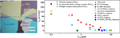
高性能p型原子薄晶体管是超硅电子器件中基于cmos的数字逻辑电路的基本元件。与n型原子薄沟道晶体管在接近量子极限的高质量半金属触点方面取得的最新突破相比,实现具有高质量触点的高性能p型类似物仍然具有挑战性,这主要是由于缺乏适当的具有费米级解钉能力的高功功能金属电极。在这里,我们证明了用无损伤转移工艺制备的半金属TiS2电极可以成为p型原子薄MoTe2晶体管的可行选择。由于其固有的大功函数(~ 5.3 eV)和TiS2/MoTe2界面上可忽略肖特基势垒的高质量接触,通道长度为500 nm的p型双层MoTe2晶体管和通道长度为800 nm的单层MoTe2晶体管分别具有100 μA/μm和68 μA/μm的高导通电流(Ion),开关比(Ion/off)大于106和68 μA/μm,开关比大于107。这样的演示将通过常见的CMOS技术实现基于mote2的单片原子薄超硅电子器件。
本文章由计算机程序翻译,如有差异,请以英文原文为准。

High-Quality P-type Contacts for Atomically Thin MoTe2 Transistors with High-Work-Function Semimetal TiS2 Electrodes

High-Quality P-type Contacts for Atomically Thin MoTe2 Transistors with High-Work-Function Semimetal TiS2 Electrodes
High-performance p-type atomically thin transistors are fundamental components in CMOS-based digital logic circuits for beyond-silicon electronics. Compared with the recent breakthrough in high-quality semimetal contacts approaching the quantum limit on n-type atomically thin channel transistors, achieving high-performance p-type analogues with high-quality contacts remains challenging, which was mainly hindered by the lack of proper high-work-function metallic electrodes with Fermi level unpinning capacity. Herein, we demonstrate that semimetal TiS2 electrodes prepared with a damage-free transfer process can be a feasible option for p-type atomically thin MoTe2 transistors. Owing to its intrinsic large work function (∼5.3 eV) and high-quality contacts with negligible Schottky barrier at the TiS2/MoTe2 interface, the scaled p-type bilayer MoTe2 transistor with 500 nm channel length and the monolayer transistor with 800 nm channel length exhibit a high on-state current (Ion) of 100 μA/μm with the on/off ratio (Ion/off) over 106 and an Ion of 68 μA/μm with the Ion/off ratio over 107, respectively. Such a demonstration will enable monolithic atomically thin MoTe2-based beyond-silicon electronics via the common CMOS technology.
求助全文
通过发布文献求助,成功后即可免费获取论文全文。 去求助
来源期刊
ACS Applied Materials & Interfaces
ACS Applied Materials & Interfaces 工程技术-材料科学:综合
CiteScore
16.00
自引率
6.30%
发文量
4978
审稿时长
1.8 months
期刊介绍: ACS Applied Materials & Interfaces is a leading interdisciplinary journal that brings together chemists, engineers, physicists, and biologists to explore the development and utilization of newly-discovered materials and interfacial processes for specific applications. Our journal has experienced remarkable growth since its establishment in 2009, both in terms of the number of articles published and the impact of the research showcased. We are proud to foster a truly global community, with the majority of published articles originating from outside the United States, reflecting the rapid growth of applied research worldwide.
×
引用
GB/T 7714-2015
复制
MLA
复制
APA
复制
导出至
BibTeX EndNote RefMan NoteFirst NoteExpress
×
提示
您的信息不完整,为了账户安全,请先补充。
现在去补充
×
提示
您因"违规操作"
具体请查看互助需知
我知道了
×
提示
确定
请完成安全验证×
copy
已复制链接
快去分享给好友吧!
我知道了
右上角分享
点击右上角分享
0
联系我们:info@booksci.cn Book学术提供免费学术资源搜索服务,方便国内外学者检索中英文文献。致力于提供最便捷和优质的服务体验。 Copyright © 2023 布克学术 All rights reserved.
京ICP备2023020795号-1
ghs 京公网安备 11010802042870号
Book学术文献互助
Book学术文献互助群
群 号:604180095
Book学术官方微信