使用 SeS2 前驱体通过化学气相沉积法生长的轻掺 Se 单层 MoS2
IF 8.2
2区 材料科学
Q1 MATERIALS SCIENCE, MULTIDISCIPLINARY
引用次数: 0
摘要
基于过渡金属二硫化物(TMDC)的二维半导体是下一代电子器件中很有前途的材料。然而,优化载流子迁移率、开/关电流比、阈值电压和最小化迟滞等挑战仍然存在。在这里,我们报道了用二硫化硒(SeS2)作为硫源,通过化学气相沉积(CVD)轻硒掺杂单层MoS2。有趣的是,与传统的MoS2相比,掺入5.5% Se (MoS1.89Se0.11)可以提高电子迁移率,这与取代掺杂增加有效质量的典型趋势相反。此外,通过控制SeS2的温度来控制Se含量,实现了带隙可调性。这种方法提供了为高级应用程序定制TMDCs属性的途径。本文章由计算机程序翻译,如有差异,请以英文原文为准。
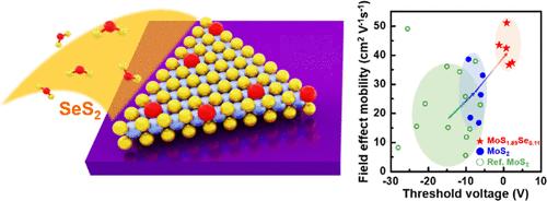
Lightly Se-Doped Monolayer MoS2 Grown by Chemical Vapor Deposition Using SeS2 Precursor
Transition metal dichalcogenide (TMDC)-based two-dimensional semiconductors are promising materials for next-generation electronic devices. However, challenges such as optimizing the carrier mobility, on/off current ratio, threshold voltage, and minimization of hysteresis remain. Herein, we report lightly Se-doped monolayer MoS2 via chemical vapor deposition (CVD) using selenium disulfide (SeS2) as a chalcogen source. Interestingly, doping with 5.5% Se (MoS1.89Se0.11) enhanced the electron mobility compared to conventional MoS2, contrary to the typical trend of increased effective mass with substitutional doping. Additionally, bandgap tunability was achieved by controlling the Se content via temperature control of SeS2. This approach offers a pathway for tailoring the properties of TMDCs for advanced applications.
求助全文
通过发布文献求助,成功后即可免费获取论文全文。
去求助
来源期刊

ACS Applied Materials & Interfaces
工程技术-材料科学:综合
CiteScore
16.00
自引率
6.30%
发文量
4978
审稿时长
1.8 months
期刊介绍:
ACS Applied Materials & Interfaces is a leading interdisciplinary journal that brings together chemists, engineers, physicists, and biologists to explore the development and utilization of newly-discovered materials and interfacial processes for specific applications. Our journal has experienced remarkable growth since its establishment in 2009, both in terms of the number of articles published and the impact of the research showcased. We are proud to foster a truly global community, with the majority of published articles originating from outside the United States, reflecting the rapid growth of applied research worldwide.
 求助内容:
求助内容: 应助结果提醒方式:


