带电薄膜可形成无掺杂欧姆金属半导体接触
IF 6.9
2区 材料科学
Q2 CHEMISTRY, PHYSICAL
引用次数: 0
摘要
欧姆触点通常是通过在金属触点下面的半导体衬底表面外部掺杂来实现的。为了避免重掺杂带来的不便,我们提出了一种利用高电荷原子层沉积(ALD) Al2O3薄膜实现欧姆Al-Si接触的替代方法。这个想法是利用ALD Al2O3的负电荷吸引孔到Si衬底表面,从而诱导p + 区域,从而导致Al/p + Si接触。结果表明,Al2O3诱导的触点不仅具有欧姆特性,而且接触电阻率低,为0.24 mΩ⋅cm2。这符合各种电子器件的要求,如光电二极管指示所提出的接触形成方法的电位。本文章由计算机程序翻译,如有差异,请以英文原文为准。

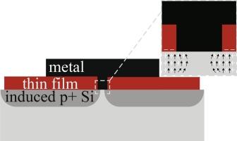
Charged thin film enables dopant free ohmic metal–semiconductor contact formation
Ohmic contacts are conventionally achieved by externally doping the surface of a semiconductor substrate underneath a metal contact. To avoid the inconveniences that come with heavy doping, we propose an alternative way of achieving an ohmic Al-Si contact utilizing a highly charged atomic layer deposited (ALD) Al2O3 thin film. The idea is to utilize the negative charge of ALD Al2O3 to attract holes towards the surface of the Si substrate and thereby induce a p+ region and consequently an Al/p+ Si contact. The results show that the Al2O3 induced contacts are not only ohmic, but also have a low contact resistivity of 0.24 mΩ⋅cm2. This matches the requirements of various electron devices such as photodiodes indicating potential for the proposed contact formation method.
求助全文
通过发布文献求助,成功后即可免费获取论文全文。
去求助
来源期刊

Applied Surface Science
工程技术-材料科学:膜
CiteScore
12.50
自引率
7.50%
发文量
3393
审稿时长
67 days
期刊介绍:
Applied Surface Science covers topics contributing to a better understanding of surfaces, interfaces, nanostructures and their applications. The journal is concerned with scientific research on the atomic and molecular level of material properties determined with specific surface analytical techniques and/or computational methods, as well as the processing of such structures.
 求助内容:
求助内容: 应助结果提醒方式:


