暴露未掺杂α-Ga2O3的氢等离子体中浅施主态的产生

IF 6.3 2区 材料科学 Q2 CHEMISTRY, PHYSICAL
A.Y. Polyakov , V.I. Nikolaev , A.A. Vasilev , E.B. Yakimov , A.I. Pechnikov , I.V. Schemerov , A.A. Romanov , L.A. Alexanyan , A.V. Chernykh , A.V. Miakonkikh , A. Kislyuk , A.V. Panichkin , S.J. Pearton
{"title":"暴露未掺杂α-Ga2O3的氢等离子体中浅施主态的产生","authors":"A.Y. Polyakov ,&nbsp;V.I. Nikolaev ,&nbsp;A.A. Vasilev ,&nbsp;E.B. Yakimov ,&nbsp;A.I. Pechnikov ,&nbsp;I.V. Schemerov ,&nbsp;A.A. Romanov ,&nbsp;L.A. Alexanyan ,&nbsp;A.V. Chernykh ,&nbsp;A.V. Miakonkikh ,&nbsp;A. Kislyuk ,&nbsp;A.V. Panichkin ,&nbsp;S.J. Pearton","doi":"10.1016/j.jallcom.2025.180291","DOIUrl":null,"url":null,"abstract":"<div><div>High concentrations, 10<sup>19</sup> cm<sup>−3</sup>, of shallow donors are created in initially semi-insulating α-Ga<sub>2</sub>O<sub>3</sub> grown on sapphire by Halide Vapor Phase Epitaxy (HVPE) after hydrogen plasma exposure. H-plasma treatment for 0.5 h at 330 °C renders the α-Ga<sub>2</sub>O<sub>3</sub> films highly conducting, with shallow donors attributed to interstitial hydrogen. There is also persistent photo capacitance to 400 K, due to the presence of a high density (10<sup>18</sup> cm<sup>−3</sup>) of deep acceptors with optical ionization threshold of 2 eV with a barrier for capture of electrons. These centers are ascribed to Ga vacancy complexes with hydrogen. The top layer of about 20 nm of the Ga<sub>2</sub>O<sub>3</sub> has a high density of these acceptors originating from surface damage created by high energy H ions. Annealing to 723 K leads to partial recovery of the initial properties, but the films retain about 10<sup>16</sup> cm<sup>−3</sup> shallow donors and some remnant centers giving rise to persistent conductivity. The deep trap spectra show electron traps at E<sub>c</sub>-0.24 eV, E<sub>c</sub>-0.82 eV, E<sub>c</sub>-1.2 eV and hole-trap-like signals due to centers with activation energy 0.2 eV and 0.9 eV. The Ga<sub>2</sub>O<sub>3</sub> after annealing exhibits low dark current and a high gain in Electron Beam Induced Current measurements. The prospects of using highly conducting hydrogenated films for low temperature fabrication of Ohmic contacts and of hydrogen treated and annealed films for use in high responsivity solar-blind photodetectors are discussed.</div></div>","PeriodicalId":344,"journal":{"name":"Journal of Alloys and Compounds","volume":"1026 ","pages":"Article 180291"},"PeriodicalIF":6.3000,"publicationDate":"2025-04-11","publicationTypes":"Journal Article","fieldsOfStudy":null,"isOpenAccess":false,"openAccessPdf":"","citationCount":"0","resultStr":"{\"title\":\"Creation of shallow donor states in hydrogen plasma exposed undoped α-Ga2O3\",\"authors\":\"A.Y. Polyakov ,&nbsp;V.I. Nikolaev ,&nbsp;A.A. Vasilev ,&nbsp;E.B. Yakimov ,&nbsp;A.I. Pechnikov ,&nbsp;I.V. Schemerov ,&nbsp;A.A. Romanov ,&nbsp;L.A. Alexanyan ,&nbsp;A.V. Chernykh ,&nbsp;A.V. Miakonkikh ,&nbsp;A. Kislyuk ,&nbsp;A.V. Panichkin ,&nbsp;S.J. Pearton\",\"doi\":\"10.1016/j.jallcom.2025.180291\",\"DOIUrl\":null,\"url\":null,\"abstract\":\"<div><div>High concentrations, 10<sup>19</sup> cm<sup>−3</sup>, of shallow donors are created in initially semi-insulating α-Ga<sub>2</sub>O<sub>3</sub> grown on sapphire by Halide Vapor Phase Epitaxy (HVPE) after hydrogen plasma exposure. H-plasma treatment for 0.5 h at 330 °C renders the α-Ga<sub>2</sub>O<sub>3</sub> films highly conducting, with shallow donors attributed to interstitial hydrogen. There is also persistent photo capacitance to 400 K, due to the presence of a high density (10<sup>18</sup> cm<sup>−3</sup>) of deep acceptors with optical ionization threshold of 2 eV with a barrier for capture of electrons. These centers are ascribed to Ga vacancy complexes with hydrogen. The top layer of about 20 nm of the Ga<sub>2</sub>O<sub>3</sub> has a high density of these acceptors originating from surface damage created by high energy H ions. Annealing to 723 K leads to partial recovery of the initial properties, but the films retain about 10<sup>16</sup> cm<sup>−3</sup> shallow donors and some remnant centers giving rise to persistent conductivity. The deep trap spectra show electron traps at E<sub>c</sub>-0.24 eV, E<sub>c</sub>-0.82 eV, E<sub>c</sub>-1.2 eV and hole-trap-like signals due to centers with activation energy 0.2 eV and 0.9 eV. The Ga<sub>2</sub>O<sub>3</sub> after annealing exhibits low dark current and a high gain in Electron Beam Induced Current measurements. The prospects of using highly conducting hydrogenated films for low temperature fabrication of Ohmic contacts and of hydrogen treated and annealed films for use in high responsivity solar-blind photodetectors are discussed.</div></div>\",\"PeriodicalId\":344,\"journal\":{\"name\":\"Journal of Alloys and Compounds\",\"volume\":\"1026 \",\"pages\":\"Article 180291\"},\"PeriodicalIF\":6.3000,\"publicationDate\":\"2025-04-11\",\"publicationTypes\":\"Journal Article\",\"fieldsOfStudy\":null,\"isOpenAccess\":false,\"openAccessPdf\":\"\",\"citationCount\":\"0\",\"resultStr\":null,\"platform\":\"Semanticscholar\",\"paperid\":null,\"PeriodicalName\":\"Journal of Alloys and Compounds\",\"FirstCategoryId\":\"88\",\"ListUrlMain\":\"https://www.sciencedirect.com/science/article/pii/S0925838825018493\",\"RegionNum\":2,\"RegionCategory\":\"材料科学\",\"ArticlePicture\":[],\"TitleCN\":null,\"AbstractTextCN\":null,\"PMCID\":null,\"EPubDate\":\"\",\"PubModel\":\"\",\"JCR\":\"Q2\",\"JCRName\":\"CHEMISTRY, PHYSICAL\",\"Score\":null,\"Total\":0}","platform":"Semanticscholar","paperid":null,"PeriodicalName":"Journal of Alloys and Compounds","FirstCategoryId":"88","ListUrlMain":"https://www.sciencedirect.com/science/article/pii/S0925838825018493","RegionNum":2,"RegionCategory":"材料科学","ArticlePicture":[],"TitleCN":null,"AbstractTextCN":null,"PMCID":null,"EPubDate":"","PubModel":"","JCR":"Q2","JCRName":"CHEMISTRY, PHYSICAL","Score":null,"Total":0}
引用次数: 0

摘要

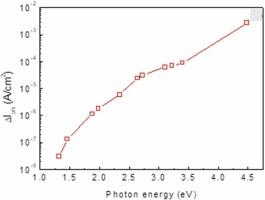
通过卤化物气相外延(HVPE)在蓝宝石表面生长的α-Ga2O3,在氢等离子体暴露后产生了高浓度的1019 cm-3的浅层供体。在330℃下h等离子体处理0.5小时,α-Ga2O3薄膜具有高导电性,由于间隙氢的存在,给体较浅。由于存在高密度(1018 cm-3)的深受体,其光学电离阈值为2 eV,并具有捕获电子的屏障,因此也存在持久的光电容至400 K。这些中心被认为是Ga与氢的空位配合物。在约20nm的Ga2O3顶层,这些受体的密度很高,这些受体是由高能氢离子造成的表面损伤引起的。退火至723 K时,薄膜部分恢复了初始性质,但仍保留了约1016 cm-3的浅层供体和一些残余中心,从而产生了持久的导电性。深阱能谱显示出Ec-0.24 eV、Ec-0.82 eV和Ec-1.2 eV的电子陷阱,以及由活化能为0.2 eV和0.9 eV的中心产生的类似空穴陷阱的信号。退火后的Ga2O3在电子束感应电流测量中表现出低暗电流和高增益。讨论了高导电性氢化薄膜用于低温制造欧姆触点以及氢处理和退火薄膜用于高响应性太阳盲光电探测器的前景。
本文章由计算机程序翻译,如有差异,请以英文原文为准。

Creation of shallow donor states in hydrogen plasma exposed undoped α-Ga2O3

Creation of shallow donor states in hydrogen plasma exposed undoped α-Ga2O3
High concentrations, 1019 cm−3, of shallow donors are created in initially semi-insulating α-Ga2O3 grown on sapphire by Halide Vapor Phase Epitaxy (HVPE) after hydrogen plasma exposure. H-plasma treatment for 0.5 h at 330 °C renders the α-Ga2O3 films highly conducting, with shallow donors attributed to interstitial hydrogen. There is also persistent photo capacitance to 400 K, due to the presence of a high density (1018 cm−3) of deep acceptors with optical ionization threshold of 2 eV with a barrier for capture of electrons. These centers are ascribed to Ga vacancy complexes with hydrogen. The top layer of about 20 nm of the Ga2O3 has a high density of these acceptors originating from surface damage created by high energy H ions. Annealing to 723 K leads to partial recovery of the initial properties, but the films retain about 1016 cm−3 shallow donors and some remnant centers giving rise to persistent conductivity. The deep trap spectra show electron traps at Ec-0.24 eV, Ec-0.82 eV, Ec-1.2 eV and hole-trap-like signals due to centers with activation energy 0.2 eV and 0.9 eV. The Ga2O3 after annealing exhibits low dark current and a high gain in Electron Beam Induced Current measurements. The prospects of using highly conducting hydrogenated films for low temperature fabrication of Ohmic contacts and of hydrogen treated and annealed films for use in high responsivity solar-blind photodetectors are discussed.
求助全文
通过发布文献求助,成功后即可免费获取论文全文。 去求助
来源期刊
Journal of Alloys and Compounds
Journal of Alloys and Compounds 工程技术-材料科学:综合
CiteScore
11.10
自引率
14.50%
发文量
5146
审稿时长
67 days
期刊介绍: The Journal of Alloys and Compounds is intended to serve as an international medium for the publication of work on solid materials comprising compounds as well as alloys. Its great strength lies in the diversity of discipline which it encompasses, drawing together results from materials science, solid-state chemistry and physics.
×
引用
GB/T 7714-2015
复制
MLA
复制
APA
复制
导出至
BibTeX EndNote RefMan NoteFirst NoteExpress
×
提示
您的信息不完整,为了账户安全,请先补充。
现在去补充
×
提示
您因"违规操作"
具体请查看互助需知
我知道了
×
提示
确定
请完成安全验证×
copy
已复制链接
快去分享给好友吧!
我知道了
右上角分享
点击右上角分享
0
联系我们:info@booksci.cn Book学术提供免费学术资源搜索服务,方便国内外学者检索中英文文献。致力于提供最便捷和优质的服务体验。 Copyright © 2023 布克学术 All rights reserved.
京ICP备2023020795号-1
ghs 京公网安备 11010802042870号
Book学术文献互助
Book学术文献互助群
群 号:604180095
Book学术官方微信