利用光电发射电子显微镜成像p-n结

IF 9.1 1区 材料科学 Q1 CHEMISTRY, MULTIDISCIPLINARY
Elizaveta Pyatenko, Shunsuke Nozawa, Keiki Fukumoto
{"title":"利用光电发射电子显微镜成像p-n结","authors":"Elizaveta Pyatenko, Shunsuke Nozawa, Keiki Fukumoto","doi":"10.1021/acs.nanolett.5c00513","DOIUrl":null,"url":null,"abstract":"We propose a method to visualize the modification of the band alignment and depletion layer structure of p–n junctions under device operation. The cross-section of the p–n interface of a GaAs backward tunnel diode was directly observed by operando photoemission electron microscopy (PEEM) under forward and reverse bias operation. In addition to obtaining the external voltage dependent energy band alignment, further spectral signatures were observed in the n-type region, which provided evidence of the tunneling of electrons under reverse bias. Moreover, the PEEM images allowed us to directly visualize the depletion layer and its widening under increasing reverse bias voltages. This method can straightforwardly be applied to any semiconductor material for a thorough understanding of the electronic structure at the interface, leading to improved efficiency and device performance.","PeriodicalId":53,"journal":{"name":"Nano Letters","volume":"211 1","pages":""},"PeriodicalIF":9.1000,"publicationDate":"2025-04-08","publicationTypes":"Journal Article","fieldsOfStudy":null,"isOpenAccess":false,"openAccessPdf":"","citationCount":"0","resultStr":"{\"title\":\"Imaging p–n Junctions Using Operando Photoemission Electron Microscopy\",\"authors\":\"Elizaveta Pyatenko, Shunsuke Nozawa, Keiki Fukumoto\",\"doi\":\"10.1021/acs.nanolett.5c00513\",\"DOIUrl\":null,\"url\":null,\"abstract\":\"We propose a method to visualize the modification of the band alignment and depletion layer structure of p–n junctions under device operation. The cross-section of the p–n interface of a GaAs backward tunnel diode was directly observed by operando photoemission electron microscopy (PEEM) under forward and reverse bias operation. In addition to obtaining the external voltage dependent energy band alignment, further spectral signatures were observed in the n-type region, which provided evidence of the tunneling of electrons under reverse bias. Moreover, the PEEM images allowed us to directly visualize the depletion layer and its widening under increasing reverse bias voltages. This method can straightforwardly be applied to any semiconductor material for a thorough understanding of the electronic structure at the interface, leading to improved efficiency and device performance.\",\"PeriodicalId\":53,\"journal\":{\"name\":\"Nano Letters\",\"volume\":\"211 1\",\"pages\":\"\"},\"PeriodicalIF\":9.1000,\"publicationDate\":\"2025-04-08\",\"publicationTypes\":\"Journal Article\",\"fieldsOfStudy\":null,\"isOpenAccess\":false,\"openAccessPdf\":\"\",\"citationCount\":\"0\",\"resultStr\":null,\"platform\":\"Semanticscholar\",\"paperid\":null,\"PeriodicalName\":\"Nano Letters\",\"FirstCategoryId\":\"88\",\"ListUrlMain\":\"https://doi.org/10.1021/acs.nanolett.5c00513\",\"RegionNum\":1,\"RegionCategory\":\"材料科学\",\"ArticlePicture\":[],\"TitleCN\":null,\"AbstractTextCN\":null,\"PMCID\":null,\"EPubDate\":\"\",\"PubModel\":\"\",\"JCR\":\"Q1\",\"JCRName\":\"CHEMISTRY, MULTIDISCIPLINARY\",\"Score\":null,\"Total\":0}","platform":"Semanticscholar","paperid":null,"PeriodicalName":"Nano Letters","FirstCategoryId":"88","ListUrlMain":"https://doi.org/10.1021/acs.nanolett.5c00513","RegionNum":1,"RegionCategory":"材料科学","ArticlePicture":[],"TitleCN":null,"AbstractTextCN":null,"PMCID":null,"EPubDate":"","PubModel":"","JCR":"Q1","JCRName":"CHEMISTRY, MULTIDISCIPLINARY","Score":null,"Total":0}
引用次数: 0

摘要

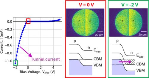
我们提出了一种方法来可视化在器件操作下p-n结的带对准和耗尽层结构的改变。利用光电显微镜(PEEM)直接观察了GaAs反向隧道二极管在正向和反向偏压下的p-n界面截面。除了获得外部电压相关的能带对准外,在n型区域观察到进一步的光谱特征,这为反向偏压下电子隧穿提供了证据。此外,PEEM图像使我们能够直接看到耗尽层及其在反向偏置电压增加下的加宽。这种方法可以直接应用于任何半导体材料,以彻底了解界面上的电子结构,从而提高效率和器件性能。
本文章由计算机程序翻译,如有差异,请以英文原文为准。

Imaging p–n Junctions Using Operando Photoemission Electron Microscopy

Imaging p–n Junctions Using Operando Photoemission Electron Microscopy
We propose a method to visualize the modification of the band alignment and depletion layer structure of p–n junctions under device operation. The cross-section of the p–n interface of a GaAs backward tunnel diode was directly observed by operando photoemission electron microscopy (PEEM) under forward and reverse bias operation. In addition to obtaining the external voltage dependent energy band alignment, further spectral signatures were observed in the n-type region, which provided evidence of the tunneling of electrons under reverse bias. Moreover, the PEEM images allowed us to directly visualize the depletion layer and its widening under increasing reverse bias voltages. This method can straightforwardly be applied to any semiconductor material for a thorough understanding of the electronic structure at the interface, leading to improved efficiency and device performance.
求助全文
通过发布文献求助,成功后即可免费获取论文全文。 去求助
来源期刊
Nano Letters
Nano Letters 工程技术-材料科学:综合
CiteScore
16.80
自引率
2.80%
发文量
1182
审稿时长
1.4 months
期刊介绍: Nano Letters serves as a dynamic platform for promptly disseminating original results in fundamental, applied, and emerging research across all facets of nanoscience and nanotechnology. A pivotal criterion for inclusion within Nano Letters is the convergence of at least two different areas or disciplines, ensuring a rich interdisciplinary scope. The journal is dedicated to fostering exploration in diverse areas, including: - Experimental and theoretical findings on physical, chemical, and biological phenomena at the nanoscale - Synthesis, characterization, and processing of organic, inorganic, polymer, and hybrid nanomaterials through physical, chemical, and biological methodologies - Modeling and simulation of synthetic, assembly, and interaction processes - Realization of integrated nanostructures and nano-engineered devices exhibiting advanced performance - Applications of nanoscale materials in living and environmental systems Nano Letters is committed to advancing and showcasing groundbreaking research that intersects various domains, fostering innovation and collaboration in the ever-evolving field of nanoscience and nanotechnology.
×
引用
GB/T 7714-2015
复制
MLA
复制
APA
复制
导出至
BibTeX EndNote RefMan NoteFirst NoteExpress
×
提示
您的信息不完整,为了账户安全,请先补充。
现在去补充
×
提示
您因"违规操作"
具体请查看互助需知
我知道了
×
提示
确定
请完成安全验证×
copy
已复制链接
快去分享给好友吧!
我知道了
右上角分享
点击右上角分享
0
联系我们:info@booksci.cn Book学术提供免费学术资源搜索服务,方便国内外学者检索中英文文献。致力于提供最便捷和优质的服务体验。 Copyright © 2023 布克学术 All rights reserved.
京ICP备2023020795号-1
ghs 京公网安备 11010802042870号
Book学术文献互助
Book学术文献互助群
群 号:604180095
Book学术官方微信